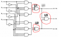
Hi to everyone I would apperciave everyones help, I have an project in Fundamental of logic design, I've done all of it expect the EXPERIMENTAL BOARD with series number can anyone tell me how to do it ?
Dear MrChips am not asking to do my homework am asking help for this thing .
If you can help I would apperciate couse this asnwer didn't help me at all :]
Dear MrChips am not asking to do my homework am asking help for this thing .
If you can help I would apperciate couse this asnwer didn't help me at all :]
First you have to change U1 U2 and U3 to something easier for u to understand.
Let's assume the 3 inputs of U1 are A, B and C and the output is (A>B).
(A>B) = A' + B' +C' = (A.B.C)' So U1 & U2 are actually 3-input NAND gates.
Applying the same method, U3 is 2-input NOR gate.
Then you can google for TTL inverter, TTL 2-input NOR. TTL 2-input NAND and TTL 3-input NAND gates. Get the chip numbers and and their datasheets. Put the pin # onto your schematic as well as the part numbers. Then you can start connecting your Experiment Board...
First you have to change U1 U2 and U3 to something easier for u to understand.
Let's assume the 3 inputs of U1 are A, B and C and the output is (A>B).
(A>B) = A' + B' +C' = (A.B.C)' So U1 & U2 are actually 3-input NAND gates.
Applying the same method, U3 is 2-input NOR gate.
Then you can google for TTL inverter, TTL 2-input NOR. TTL 2-input NAND and TTL 3-input NAND gates. Get the chip numbers and and their datasheets. Put the pin # onto your schematic as well as the part numbers. Then you can start connecting your Experiment Board...

 Facebook
 Google
 GitHub
 Linkedin