 Facebook
 Google
 GitHub
 Linkedin
Hi,
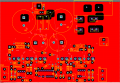
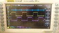
I am designing a push-pull converter.
I attached the schematic, PCB layout, Vgs, Vds and ICs voltage supply.
my problem is that I have got voltage spikes on MOSFETs.
- I have used 2 PCB layers and top layer as a GND plane.
- I have used decoupling capacitors across the ICs.
- I have used RC snubber.
but the problem still exists.
Attachments
-
 161.8 KB Views: 8
 -
 129.9 KB Views: 8
 -
 610 KB Views: 8
 -
 429.5 KB Views: 8
 -
 610 KB Views: 8
 -
 101.4 KB Views: 7
 -
 429.5 KB Views: 8
 -
 101.4 KB Views: 8
 -
 106.6 KB Views: 8


