ground plane
- Thread starter Dadu@
- Start date
Scroll to continue with content
ronsimpson
- Joined Oct 7, 2019
- 3,037
Good engineering practice, which reduces several types of noise.
Making a PCB is not an additive process. They do not add copper! They eat away copper with strong chemicals. The more copper you can leave on the PCB the less chemicals to pollute.
Making a PCB is not an additive process. They do not add copper! They eat away copper with strong chemicals. The more copper you can leave on the PCB the less chemicals to pollute.
Noise on the ground line due to ground currents can be a problem in many circuits.
This noise is the difference in the ground voltage between different parts of the circuit due to signals flowing through the ground impedance, both resistive and inductive,
A ground plane minimizes the ground impedance, and thus the ground noise.
Designers sometimes use a plane for the circuit power rail(s) for the same reason.
A ground plane may not always be needed, depending upon the circuit sensitivity to noise and the circuit frequencies involved, but you don't want to find that out after you've designed and built the board.
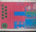
When I look at the any PCB layout I don't understand which terminal of the component is connected to the ground plane
For example Image from link https://pcbdesignworld.com/article/pcb-grounding-techniques-that-every-designer-should-know

Is that one terminal of the P3 block is connecting to the terminal of the other component while the other terminal is connecting to ground?
Is that two terminal of the R2 is connecting to the terminal of the Q1 component while the other terminal is connecting to ground?
I guess that the large amount of blue color visible in the PCB is the ground.
How do you know which one is connected to ground and which is connecting to the other component's terminal
For example Image from link https://pcbdesignworld.com/article/pcb-grounding-techniques-that-every-designer-should-know

Is that one terminal of the P3 block is connecting to the terminal of the other component while the other terminal is connecting to ground?
Is that two terminal of the R2 is connecting to the terminal of the Q1 component while the other terminal is connecting to ground?
I guess that the large amount of blue color visible in the PCB is the ground.
How do you know which one is connected to ground and which is connecting to the other component's terminal
ronsimpson
- Joined Oct 7, 2019
- 3,037
All the CAD programs I use have a function which lights up all pins connected to a node by name. I can ask for all grounds to be highlighted.
The resolution is low so I cannot see the therminals or where C3 connects.
I used "paint" to change all connected blue to red and it might be better for viewing.

The resolution is low so I cannot see the therminals or where C3 connects.
I used "paint" to change all connected blue to red and it might be better for viewing.

Last edited:
ronsimpson
- Joined Oct 7, 2019
- 3,037
If you set the "thermal connection line width" to much larger it will be easy to see. In post #8, see how thin the lines are (bottom left corner).
I solder in a way where thermals are not helpful. I do not use them. I understand hand soldering is harder without.
I solder in a way where thermals are not helpful. I do not use them. I understand hand soldering is harder without.
@nsaspook i liked your second image
There are many tools available, Which CAD tool do you use for PCB design
@ronsimpson Thank you for nice advice
There are many tools available, Which CAD tool do you use for PCB design
@ronsimpson Thank you for nice advice
Fusion360/Eaglecad but most programs are capable of good results with experience on the design platform.@nsaspook i liked your second image
There are many tools available, Which CAD tool do you use for PCB design
@ronsimpson Thank you for nice advice


3-phase motor drive system with MODBUS and other interfaces. Proper grounds/ground planes and signal integrity factors (device placement, routing, 4 layers) are important on a board with mixed digital, analog and power interfaces.
Eagle is still 'free' for limited 2 layer designs.
https://www.autodesk.com/products/eagle/free-download
Last edited:
ronsimpson
- Joined Oct 7, 2019
- 3,037
I used Eagle for years but move to KiCAD, which is free.Which CAD tool do you use for PCB design
A ground plane can remove heat and at the same time can reduce signal interference on nearby circuit components.
When signal strength is much higher than necessary, consider a simple filter to both attenuate and remove harmonics.
It may be useful to draw out the results after probing. This type of drawing involves the board micro field diagrams are directional like the probe orientation with regard to the flat ground plane.
Rather than putting priority on manipulating trace let placement of components reduce issues with parasitic inductance then improve routing where necessary. When you isolate the location of the problems keep your focus on that specific location then zoom out to see where your modification takes you. Often it is only a small change that corrects an issue. It is always preferred to solve issues before all the parts soldered in place but desoldering and rework is common.
Last edited:
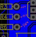
I don't understand what you are indicating. you made the arrow and you wrote yes and no so I don't know what you are indicating
Your through-hole copper pads are the purplish color that you can barely at the perimeter of each pad.I don't understand what you are indicating. you made the arrow and you wrote yes and no so I don't know what you are indicating
Your through-hole "solder mask layer" is grey (majority of the pad seen). Solder mask covers the whole side of the PCB EXCEPT where solder mask is shown.
So, anywhere that the blue ground plane touches that purplish edge of a pad means the pad is connected to the ground plane. This is where I have the word "yes".
Your software creates "thermal spokes" when the "copper pour" is used to create the ground plane on the round pads. For some reason, pad P2 is connected to the ground plane with one thin copper trace (lower right corner of the pad) but there are no thermal spokes on this pad.
Pads that are only connected to a single trace (like the one labelled "no" above) and that trace does not connect to ground plane are not connected to ground plane. That is, the pad is surrounded by black space.


