 Facebook
 Google
 GitHub
 Linkedin
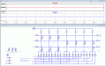
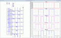
yes i got it that to implement all the states and show the functioning of full adder i need to change the test voltages of a b and cin but how do i go about doing that? i dont have any clue regarding it. So far i have only worked with .DC mostly. Can u please help me with that?hi 680,
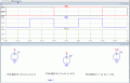
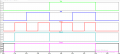
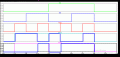
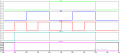
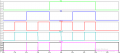
The point I am making is that the test pattern of A, B CYi , of the LTS is set to prove the OR function.
In order to check the full adder operation you need to modify the A,B CYin test voltages , so that you get all the possible input states.
Do you follow what I am saying.
E
Full Adder in Ltspice
- Thread starter omkarshinde680
- Start date


| Thread starter | Similar threads | Forum | Replies | Date |
|---|---|---|---|---|
|
|
Need help with 74ls193 | Digital Design | 12 | |
|
|
Adding -A-B in a Full Adder | Homework Help | 2 | |
|
|
Logic circuit projects issue | Homework Help | 69 | |
| R | Designing a logic circuit using a full adder? | Homework Help | 7 | |
| N | Question about parallel FULL ADDER | Homework Help | 3 |


