Full adder design

WBahn

Joined Mar 31, 2012
33,192
There are a couple of ways to proceed. First, have you been through the exercise of implementing an AND, and OR, and a NOT using only NAND gates? If so, then you could just implement your logic using 2-input AND, OR, and NOT gates and then replace each gate with its NAND implementation. This is very straight forward because going from a multi-input AND or OR to an equivalent that uses just 2-input ANDs or ORs is trivial.

Another way to do it is to draw the circuit and then use bubble logic to transform it into just NAND gates. SOP form lends itself to this.
 

Brownout

Joined Jan 10, 2012
2,390
You've constructed the expressions using the combinations of inputs that produce the desired output. Now, what about using the combinations of inputs that produce the compliment output and inverting it? Won't that give you the same thing? You can start by going back to your karnaugh maps and getting the expressions for the compliment. Can you guess an easy way to do that?
 

WBahn

Joined Mar 31, 2012
33,192
For the Cout, you are all but there. You already have all of the AND terms with just two inputs. You now just need to split the 3-input OR into two 2-input ORs. Once you have done that, you just need to apply DeMorgans (via bubble logic is the easiest) and you will end up with six two-input NAND gates, one of which is wired as an inverter.

For the other one, you might recognize that as the checkerboard pattern associated with a particular type of logic function and realize you need two of those and that each can be implemented using four two-input NAND gates.

So your solution can be done in no more than fourteen two-input NAND gates. I doubt it can be done in less, but I don't have a proof of that.
 

Thread Starter

renegadegas

Joined Dec 2, 2012
89
Hello,

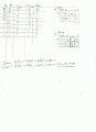
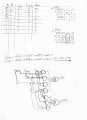
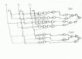
I have attached the full adder circuit i designed.
I have also included the 2 input NAND implementation of the full
adder circuit.

Please check to see if i'm on the right track so i can go ahead
and cut out the unnecessary NAND gates from the design.

Thank you.
 

Attachments

WBahn

Joined Mar 31, 2012
33,192
Ah. Now your PM makes a bit more sense.

I haven't walked through the logic in detail, but it looks like it has a good chance of being correct.

But YOU should walk through it and see if it is correct! One of the skills that you HAVE to develop is the ability to verify the correctness of your own work.
 
Top