Facebook
 Google
 GitHub
 Linkedin
A few days ago, I purchased an old monitor off eBay for a separate project. I chose the cheapest monitor I could find, but it turned out that the LCD itself was not broken, which I expected, but instead it just did not power on. I decided to make fault finding the power supply another project to learn more.
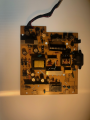
The monitor is a Dell P2210, and luckily for me a service manual exists, although it isn't the best. The service manual seems to have originally been a Word document, but has been exported to a PDF so some of the schematics are cut off and there are a bunch of pages that have all the text set to white so they look blank. The service manual is attached to this post. I have also attached some pictures of the power supply.
I started by doing a visual inspection of the power supply. There is no obvious dry solder joints or cracks, no bulging capacitors, no burn marks and no soot anywhere. There is also no smell of any burning on any of the components.
I then checked the fuses (F850, F852) and the thermistor (RT850) which seem to be OK.
On the power supply there are three different voltage rails, 16V, 12V and 5V. The 16V rail powers the CCFL backlight transformer. The 12V rail powers an audio barrel jack for some external audio device, and the 5V rail is what powers the mainboard. None of these three rails have any power which leads me to believe the issue is on the high-voltage side.
This is where I started following some of the troubleshooting steps of the service manual. I have copied and pasted them below as they are within some of the pages that have white text. They seem to have originally been formatted in a flowchart arrangement, but as I have to copy and paste the text, that formatting is lost.
As I mentioned before due to the weird formatting, the schematics of the power supply board are slightly cut off so attached is also a picture of both schematics connected together in full.

Pin 8 is the high voltage pin. This pin essentially powers the chip as it uses this to charge a "bulk capactior", attached to
Pin 7 in NC. Pin 6 is

Pins 5 and 3 are GND. Pin 4 is connected to the optocoupler
I tried measuring this pin and there seems to be no square wave on the output.
I mentioned that when

But rather than then staying a stable voltage, it seems to repeat this spike over and over again, like it's hiccuping. It mentions in the datasheet:
When I was reading Vcc with my multimeter, I did read voltages in the 20s, but my oscilliscope said it has a max reading of only about 7 or so volts. Not sure who to believe as my oscilliscope is only one of the small cheap ones.
I have to be honest, I am struggling to remember every other little thing I tested but I wouldn't say they gave me anything that important. If I had to take a guess, I would say it is something to do with this PWM controller as there is no square wave driving the MOSFET, therefore no current induced in the transformer, but why the chip is not turning on I am not sure.
If I'm not at all correct I'd like to know what the problem may be, but if I'm on the right track I'd just like to know where I can potentially diagnose next to be 100% sure that is the root cause of the problem (because maybe the OVP is triggering and that may be caused by something elsewhere).
Here is both schematics of the main board together, with their respective figures. The only 2 connections I was unsure about was pins 3 and 5 of the transformer since they aren't marked on the PCB, but I would assume pin 3 is next to pin 1 and pin 5 is next to pin 6, so that's how I connected them.
View attachment full_schem.png
EDIT: I should add that I removed
Description of FIG.6:
Description of FIG.7:
Any insight is appreciated!
Thanks, Bod.
The monitor is a Dell P2210, and luckily for me a service manual exists, although it isn't the best. The service manual seems to have originally been a Word document, but has been exported to a PDF so some of the schematics are cut off and there are a bunch of pages that have all the text set to white so they look blank. The service manual is attached to this post. I have also attached some pictures of the power supply.
I started by doing a visual inspection of the power supply. There is no obvious dry solder joints or cracks, no bulging capacitors, no burn marks and no soot anywhere. There is also no smell of any burning on any of the components.
I then checked the fuses (F850, F852) and the thermistor (RT850) which seem to be OK.
On the power supply there are three different voltage rails, 16V, 12V and 5V. The 16V rail powers the CCFL backlight transformer. The 12V rail powers an audio barrel jack for some external audio device, and the 5V rail is what powers the mainboard. None of these three rails have any power which leads me to believe the issue is on the high-voltage side.
This is where I started following some of the troubleshooting steps of the service manual. I have copied and pasted them below as they are within some of the pages that have white text. They seem to have originally been formatted in a flowchart arrangement, but as I have to copy and paste the text, that formatting is lost.
As I mentioned before due to the weird formatting, the schematics of the power supply board are slightly cut off so attached is also a picture of both schematics connected together in full.
On the PWM driver board:Is there DC16V output? No.
Is there DC5V at L851? No.
Is the voltage at C854 in the range of 127V~339V? Yes, about 324VDC (powered by 240VAC).
Is the voltage at pin8 of U850 312V? Yes, although about 324VDC.
Is the voltage at pin5 of T850 120V? Sort of? There is voltage but it's 324VDC. I'm not sure where the 120 came from but it seems like the 324 is within spec so I guess it's OK.
Check Q850: Did the test in-circuit but it seems alright.
Check D852, D851: They have a lower voltage drop but I can't read the make of the diodes and it's only lower by about 0.1-0.2V so they also seem fine.
After this, I started looking more into whatIs the voltage at pin2 of U850 0.9V? No. There is no voltage on the current sensing pin.
CN852 is, and it seems to be a PWM driver for the N-channel MOSFET (Q850). The board (the schematic attached below) is controlled by the LD7575. Unless I mention otherwise, any pin that I reference about the PWM driver is going to be of CN852 (the 8 pin connector) and NOT of U850.Pin 8 is the high voltage pin. This pin essentially powers the chip as it uses this to charge a "bulk capactior", attached to
Vcc (C878 on the main power supply board), which is then used to power the chip, if I understand correctly. Once Vcc reaches a high enough voltage UVLO (on) (anywhere between 15V and 17V), the chip starts up. If Vcc gets too high (anywhere from 25V to 30V), it triggers the over voltage protection (OVP) which causes the chip to turn off. Depening on what caused the OVP to trigger, it can get stuck in a "hiccup" mode where it repeatedly tries to turn on when Vcc is greater than UVLO (on), but then triggers the OVP and turns off again.Pin 7 in NC. Pin 6 is
Vcc, which in the monitor schematic is connected to a pin of the transformer, but this just seems to be essentially using it as an inductor, like it's shown in the typical application of the LD7575:Pins 5 and 3 are GND. Pin 4 is connected to the optocoupler
I850 . Pin 2 is the current sensing pin, which is meant to have 0.9V but doesn't. Pin 1 is the square wave output that drives the mosfet. Pin 1 of U850 is connected to GND via a 100K resistor which sets the frequency of the square wave to 65KHz.I tried measuring this pin and there seems to be no square wave on the output.
I mentioned that when
Vcc hits UVLO (on) , the chip turns on and anything above can trigger the OVP and cause it to hiccup. I measured Vcc with my ocscilliscope and noticed that it was expressing this "hiccuping" behaviour. It spikes like shown in the datasheet:But rather than then staying a stable voltage, it seems to repeat this spike over and over again, like it's hiccuping. It mentions in the datasheet:
So I did try desoldering both pins 1 and 2 at first, and then pin 4 as well but it expressed the same behaviour with the pins disconnected (I continuity tested to make sure they were fully disconnected).The OVP condition, usually caused by the feedback loop opened, is not released, the Vcc will tripped the OVP level again and re-shutdown the output.
When I was reading Vcc with my multimeter, I did read voltages in the 20s, but my oscilliscope said it has a max reading of only about 7 or so volts. Not sure who to believe as my oscilliscope is only one of the small cheap ones.
I have to be honest, I am struggling to remember every other little thing I tested but I wouldn't say they gave me anything that important. If I had to take a guess, I would say it is something to do with this PWM controller as there is no square wave driving the MOSFET, therefore no current induced in the transformer, but why the chip is not turning on I am not sure.
If I'm not at all correct I'd like to know what the problem may be, but if I'm on the right track I'd just like to know where I can potentially diagnose next to be 100% sure that is the root cause of the problem (because maybe the OVP is triggering and that may be caused by something elsewhere).
Here is both schematics of the main board together, with their respective figures. The only 2 connections I was unsure about was pins 3 and 5 of the transformer since they aren't marked on the PCB, but I would assume pin 3 is next to pin 1 and pin 5 is next to pin 6, so that's how I connected them.
View attachment full_schem.png
EDIT: I should add that I removed
T850-1 from since it's the same as T850, but just a smaller footprint of transformer.Description of FIG.6:
D850 is a rectifier in which there are 4 build-in diodes, inverting AC to DC.
C854 is used to smooth the wave from rectifier. U850 is a highly integrated PWM controller. Typical start-up current for U850 is only 20 uA, When current
flow through R842/R843 gets to Pin 8 of U850, with VDD hold-up capacitor C878,
U850 is enough for starting up. When U850 begins to operate Pin5 of U850 will output square wave to drive
Q850, then the main current flow get to GND bypassing through T850, Q850. Because of the change of current flow, wires in the other side of T850 will induct current. In the same time, the current inducted by wires which connected T850 Pin 1
and Pin 3, with components of D852, R856and C878 ,will be supplied to U850 for
normal operating. When the sense voltage across the sense resistor R869, reaches the threshold
voltage around 0.85v, the output GATE drive will be turned off. Every time when the output of power supply is shorted or over loaded, the FB voltage will increase, the build-in PWM output will then be turned off. Both of two will prevent the power supply from being overheated under over loading condition. The PWM duty cycle is determined by this current sense signal and COMP, the feedback voltage,
when the voltage on pin2 reaches V-(PWMcopm) =(Vcomp-2VF)/3, A switch cycle
will be terminated immediately, Vcomp is internally clamped to a variable voltage around 0. 85 V for output power limit
When Q850 are turned off, the main current flow will be consumed through D851, C858, R854 and D853, This will prevent Q850 from being damaged under large current impulse and voltage spike.
Description of FIG.7:
D854&D855 are used to rectify the inducted current. C865 and C862 are used to
store energy when current is reversed. The parts including L852 are used to smooth the current waves that are from D854&D855, and then 16V voltage is supplied.
D880&D881 are used to rectify the inducted current . C884 is used to store energy when current is reversed. The parts Q852 is a switch and is controlled by Q853 ,and then 12V voltage is supplied.
D856 is used to rectify the inducted current. C874,C864 are used to store energy
when current is reversed. The parts including L851,and C875 are used to smooth the current waves that are from D856, and then 5V voltage is supplied.
5V supply voltage feed back to PWM controller U850 via R861, R860,and I850,I851.R859,C859 and C863 are used to control response time.
LD7575 implements an OVP function on Vcc .Whenever the Vcc voltage is higher than the OVP threshold voltage, the output gate drive circuit will be shutdown simultaneously thus to stop the switching of the power MOSFET until the next on.
Any insight is appreciated!
Thanks, Bod.
Attachments
-
2.4 MB Views: 14
-
 9.9 MB Views: 10
 -
 8.3 MB Views: 10