Eagle PCB layout design Help

Thread Starter

@vajra

Joined May 2, 2018
154
Hello everyone

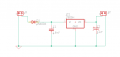
I have eagle software to design PCB. I have created circuit diagram in Eagel software it’s power supply circuit for 9v DC battery that give 5v DC and now I want to convert it into PCB layout. My aim to learn PCB designing so just spent time on the internet and started with my own example


See the image

upload_2019-2-28_16-52-22.png


1) How to convert circuit diagram into PCB layout ?

2) is it possible to make a PCB layout without making the circuit diagram schematics in Eagle?
 

pmd34

Joined Feb 22, 2014
527
Hi vjra,

1) you go to the "file" menu then "switch to board"

2) Yes you can: In the main window which lists your projects; right click on a project & "create" "new board".. you can now add components in the same way as you did in schematic mode. But you will not be able to generate a schematic from the board, and there will be no signal error checking, so its not really recommended.
 

Thread Starter

@vajra

Joined May 2, 2018
154
Hi vjra,

1) you go to the "file" menu then "switch to board"

2) Yes you can: In the main window which lists your projects; right click on a project & "create" "new board".. you can now add components in the same way as you did in schematic mode. But you will not be able to generate a schematic from the board, and there will be no signal error checking, so its not really recommended.
Hello pmd34

Thank you so much for your help

This my new circuit

upload_2019-2-28_17-54-55.png

Then I am trying to convert it into PCB layout

upload_2019-2-28_17-56-36.png


Can help me to make my first PCB layout?
 

Attachments

pmd34

Joined Feb 22, 2014
527
Hi vjra! I can try my best, though I have an older version of Eagle. (There are a lot of tutrials online for eagle which I am sure are better at explaing than me.. but here goes...)

What you now have is the components with pads (shown in green) and the wire connections that need routing (shown my the yellow lines).

The first step is to move you components, rotate them etc. around the board until you have them close together and things like conectors where you want them.. opposite sides of the board etc.

You aim ideally is to have the yellow connecting wires as short as possible between the components.

Once you have the components arranged, you can then either "auto route" or manual route them.
You are probably best using auto route first, just to see how it works.
I was cheap so I didnt get the autoroute function on mine. If you route them manually you can change track thicknesses part way along a signal, and have much more control over how things are routed, but it can be very time consuming.

This:

Seems like a reasonable tutorial for you to understand some of the things with routing a PCB.
Best of luck!
 
Top