drain current spike in full bridge inverter.

Thread Starter

rashanshr

Joined Nov 10, 2018
9
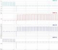
HI everyone. I have been trying to simulate a full bridge inverter using CPM2-1700-0045B mosfet with the driver with the ADuM4121 gate driver. I was able to decrease the postive voltage spike in drain by increasing the gate resistance but there still exist significant spike in the negative side as you can see in the waveform. I have a switching frequency of 2KHz. There is a difference in the PWM waveform for input and output of the driver(in attached figure). I can see a turn on delay for the gate pulse in the output of the gate driver. My Vth is 3V for the mosfet and my gate pulse amplitude(peak) is15V. I fear my mosfets are turning on before my gate pulse reaches 15V i.e mosfet is turning on during the rising edge of my gate pulse I am not sure how to confirm this.
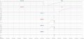
Also my gate current through the Ron(in figure) which is my gate resistance is 25.6mA which I don't think is sufficient to drive my mosfet gate that has a total gate charge of 188nC and rise time of 20ns which gives me a required gate current to be(Qtot/Trise ) if I am right(I fail to calculate the total gate current required) I have used
Ig=Ciss*V(15 volts gate voltage*switching freq) assuming total gate capacitance to be Ciss from datasheet.

Also I have been pointed out that my gate driver is slow and is causing the negative drain current spike(of peak mag 1.6A) and I know this is not good for the mosfet and I would really appreciate if anyone could help understand this problems and point me to the direction of solving these problems.

Thank you.
 

Attachments

MisterBill2

Joined Jan 23, 2018
18,461
I see nothing in the circuit to prevent both the upper and lower mosfets from being on at the same time. THAT can be the source of large problems.
 

Thread Starter

rashanshr

Joined Nov 10, 2018
9
Well you can see the gae pulse ar not high at the same time. And dont you think it will prevent the upper and lowe mosfet from turning on at the same time? If not, what kind of circuit would you need to prevent that?
 

MisterBill2

Joined Jan 23, 2018
18,461
Well you can see the gae pulse ar not high at the same time. And dont you think it will prevent the upper and lowe mosfet from turning on at the same time? If not, what kind of circuit would you need to prevent that?
Fore most FET power devices the switch off is slower than the switch on. That is what I was thinking. Just because the control switches off does not mean the device shuts off that instant.
 

MisterBill2

Joined Jan 23, 2018
18,461
so how would you suggest i correct this problem of negative spike.
First it would make sense to verify that it is the cause of the problem, because while it is usually a concern it is not always a problem, since some circuits include prevention functions. Depending on the driver circuit adding a small delay between switch off of one set and switch on of the opposite set may be simple or not. The common name for the problem is "shoot through", which may make searching for a solution work better. If you are producing the drive in software it would be a simple code addition.
 

Thread Starter

rashanshr

Joined Nov 10, 2018
9
I have a deadband between the two gate pulses. If there was a shoot through then, the spike should have been in every cycle,. However, the spikes are not regular.
 

MisterBill2

Joined Jan 23, 2018
18,461
I have a deadband between the two gate pulses. If there was a shoot through then, the spike should have been in every cycle,. However, the spikes are not regular.
You are correct about that, I think. So possibly there is a noise issue that comes from noise not directly part of this section of the circuit. Are the pulse trains generated with software, or with an actual electronic circuit?
 

Thread Starter

rashanshr

Joined Nov 10, 2018
9
The pulse train is generated using circuit components by comparing triangular wave and two 180 degree out of phase sine wave in a unipolar PWM switching. I have used an ideal behavioral source as an camparator.
 

Attachments

ebp

Joined Feb 8, 2018
2,332
Show the waveforms on a time scale that actually allows seeing detail so that the timing relationship between the large amplitude positive pulses relative to the small negative going pulses can be seen. It may be possible to see this if just once complete cycle is shown, but it may require even greater expansion. 0 to 20 ms might be adequate. If not, perhaps 5 ms to 10 ms.

My suspicion is that the negative pulses are coupling though FET capacitances.
 

Thread Starter

rashanshr

Joined Nov 10, 2018
9
I used to have a high positive spike and I got rid of those by increasing the gate resistance to 250ohms. however the negative spike are still there( of around 1.6Ams). I am not sure how the spike will affect the mosfet(Id for the mosfet is 70A). You can also see a big spike in S3 image somewhere around 108ms in the drain cureent. the next big spike is around 4A and then 1.4A. the 1.4A spikes are present in every cycle.

The reverse recovery of the body diode might have caused it but is there a way to minimiaze it? I tried increasing the gate resistance and swtching frequency.
 

Attachments

MisterBill2

Joined Jan 23, 2018
18,461
I used to have a high positive spike and I got rid of those by increasing the gate resistance to 250ohms. however the negative spike are still there( of around 1.6Ams). I am not sure how the spike will affect the mosfet(Id for the mosfet is 70A). You can also see a big spike in S3 image somewhere around 108ms in the drain cureent. the next big spike is around 4A and then 1.4A. the 1.4A spikes are present in every cycle.

The reverse recovery of the body diode might have caused it but is there a way to minimiaze it? I tried increasing the gate resistance and swtching frequency.

The spike seems to be synchronous with the start of the negative slope in trace #2, whatever part of the circuit that is. So perhaps that area merits some examination.
 

ebp

Joined Feb 8, 2018
2,332
I think the difference in amplitude of the spikes is probably nothing more than an artifact of the the time step used for the simulation. Alternatively, it my be "aliasing" between the "actual" waveform and the pixels of the display. In S1.jpg the spikes are a single pixel wide, so to be in proportion in S3 they would have to be a tiny fraction of a pixel wide, which is of course impossible. This is the same issue that happens with digital oscilloscopes.

I don't have time to look at this closely right now.
 

Thread Starter

rashanshr

Joined Nov 10, 2018
9
I think the difference in amplitude of the spikes is probably nothing more than an artifact of the the time step used for the simulation. Alternatively, it my be "aliasing" between the "actual" waveform and the pixels of the display. In S1.jpg the spikes are a single pixel wide, so to be in proportion in S3 they would have to be a tiny fraction of a pixel wide, which is of course impossible. This is the same issue that happens with digital oscilloscopes.

I don't have time to look at this closely right now.
Thanks for the input.
 

MisterBill2

Joined Jan 23, 2018
18,461
I think the difference in amplitude of the spikes is probably nothing more than an artifact of the the time step used for the simulation. Alternatively, it my be "aliasing" between the "actual" waveform and the pixels of the display. In S1.jpg the spikes are a single pixel wide, so to be in proportion in S3 they would have to be a tiny fraction of a pixel wide, which is of course impossible. This is the same issue that happens with digital oscilloscopes.

I don't have time to look at this closely right now.
Those spikes being an artifact instead of real is interesting. The frequency is low enough hat the waveform could easily be seen on an analog scope, even an older one, if such is available.
OR, you can try magnifying the area of the trace with the spike just a bit more. That may make a difference, if it is an artifact.
 
Top