DIY Double sided design and assembly?

Thread Starter

spinnaker

Joined Oct 29, 2009
7,830
I have always done single sided boards i my projects. I would like to try my hand at double sided boards for my next project.

Mainly I have a question on how to solder a run that is on the component side of the board for though hole components. Something like a resistor would be fairly easy to solder on both sides of the board but what about a chip? Or more specifically a socket for a chip?

If I am doing DIY boards, how would I solder both sides of a pin going to a socket? If I solder the outside of the pin, will the solder flow all around the pine?
 

dl324

Joined Mar 30, 2015
16,916
Layout your board with two layers, using vias to connect between top and bottom layers. Use a wire in each via soldered from top and bottom. Everything else is only soldered from the bottom.
 

Travm

Joined Aug 16, 2016
363
I'm definitely not an expert on this, but all I've ever done are double sided boards, and I have no trouble putting sockets resistors caps on either side. Only caveat is they have to be pads on both sides and copper through holes. Clean parts and board is like the solder just knows what to do.

Edit, I just re read your post, diy boards, I have no idea how you would get the solder to the other side. I would not expect it to flow without copper in the hole. Drill the holes oversized and run wire thru each?
 
Last edited:

Sensacell

Joined Jun 19, 2012
3,444
No-worth-the-trouble!

Having to align the layers perfectly, then solder on both sides- it's really a pain, and you end up with an unreliable unit in the end.
 

MaxHeadRoom

Joined Jul 18, 2013
28,684
Have a look at sending your boards to https://jlcpcb.com/ and you will bet really good boards back. I have started to use them and they are very cheap.
.
The price for 10 boards is $2.00 but $17.00 shipping, like a few of the cheap PCB suppliers, they have stopped using Chinese or Hong Kong post, DHL or UPS only.
There are a couple of exceptions if a search is done.
Max.
 

Thread Starter

spinnaker

Joined Oct 29, 2009
7,830
Layout your board with two layers, using vias to connect between top and bottom layers. Use a wire in each via soldered from top and bottom. Everything else is only soldered from the bottom.

So add a pad next to the chip pad. Add on ad the end of the run, snake a wire between them? That was one of the things I was thinking before I posted the OP.
 

mcgyvr

Joined Oct 15, 2009
5,394
Are you asking about through hole components?
Just apply solder to the pin/pad on both sides to connect layers..
Its not difficult at all..
And run a trimmed off resistor lead or wire through any vias to connect them.

If SMT chips then check the fanout option in your design software to place a through/via hole just off from each SMT pad and solder a wire through it to connect the layers..
I've seen people also use pop rivets to connect the layers but they take up more room..
 

WBahn

Joined Mar 31, 2012
30,051
I have always done single sided boards i my projects. I would like to try my hand at double sided boards for my next project.

Mainly I have a question on how to solder a run that is on the component side of the board for though hole components. Something like a resistor would be fairly easy to solder on both sides of the board but what about a chip? Or more specifically a socket for a chip?

If I am doing DIY boards, how would I solder both sides of a pin going to a socket? If I solder the outside of the pin, will the solder flow all around the pine?
Some of the first DIY boards I did were double sided and the key to using component leads as vias is just to examine the components before you do the layout and decide which ones you are confident in having adequate access to solder both sides of the board at assembly time. Sometimes this depends on what other components have already been assembled, so keep that in mind, too.

Where you need vias that can't be serviced by a component lead, use scrap component leads. What I would do as my first assembly step was set the board up on pennies in the corners and drop scrap leads into each via hole. Since I would know after layout how many such vias I had, I would set aside exactly that many scrap leads to make sure that I got them all (though this does assume that I actually put each lead into a via hole and not a component hole -- sadly a bad assumption on one occasion). Then I would solder and snip them working from front to back (so that the unsnipped leads weren't in the way). I would then flip the board over, keeping it up on the pennies, and solder the other side. Since I would try to snip the leads so that they stuck up right about the height of the penny I didn't need to worry about the solder on the original side melting and the lead dropping out. This approach worked very well for me -- I don't recall any failures of any of my boards even though some of them were in use for several years.
 

Thread Starter

spinnaker

Joined Oct 29, 2009
7,830
No-worth-the-trouble!

Having to align the layers perfectly, then solder on both sides- it's really a pain, and you end up with an unreliable unit in the end.

I might be ahaed of the game on that one. I pre CNC drill the boards. I then do the toner transfer method. I transfer to tax paper or parchment paper so I have a translucent medium to work with. So the holes make a built in line up for the transfer.

But with the vias I am wondering if double sided is worth it. Most of my designs don't have a whole lot of components on a board. And I do pretty darn well with board layout that minimizes any jumpers. I considered double sided to totally eliminate any jumpers. But if I need to add vias then I am back in the same boat and maybe even worse off.

P.S. I don't isolation mill because I don't like the results. And I don't buy the lack of chemicals a benefit since milling creates all of that dust which is probably far more dangerous.
 

MrChips

Joined Oct 2, 2009
30,802
DIY double-sided PCB is doable, but as others have said, is it worth the trouble?
If you want to give it a try, here are some tips.

1) Think about the component side when doing the layout.
2) Avoid running a trace under an IC to a pin.
3) You cannot use IC sockets except the free standing socket pins that will allow you to solder from the component side.
4) All vias must be accessible.
5) Pay attention to large components such as vertical standing electrolytic capacitors, connectors, headers, coin cell holders, etc. if you need to solder from the component side.
 

Travm

Joined Aug 16, 2016
363
I might be ahaed of the game on that one. I pre CNC drill the boards. I then do the toner transfer method. I transfer to tax paper or parchment paper so I have a translucent medium to work with. So the holes make a built in line up for the transfer.

But with the vias I am wondering if double sided is worth it. Most of my designs don't have a whole lot of components on a board. And I do pretty darn well with board layout that minimizes any jumpers. I considered double sided to totally eliminate any jumpers. But if I need to add vias then I am back in the same boat and maybe even worse off.

P.S. I don't isolation mill because I don't like the results. And I don't buy the lack of chemicals a benefit since milling creates all of that dust which is probably far more dangerous.
I have no practical experience with it but electroless copper deposition is the best way to do 2 sided boards. I have done lots of research on the topic and it seems some are having success at home with it. With cheap Chinese board houses it's hard to justify the effort for me to do this at home.
 

jpanhalt

Joined Jan 18, 2008
11,087
@spinnaker
Sorry to be so late replying -- couldn't find my tripod and hands are too shaky.

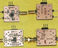
I agree about buy rather than make, unless it is one-off, and you need them in a hurry. I was in that situation awhile back, so I made several versions of some boards, each is about 1" square. Front and back are shown, flipped left to right. I use a small (e.g., #72) carbide bit and 24 awg wire to make vias. That drill allows short pieces of wire to stay in place by friction. Solder and clip flush (if needed). I like to leave a little nubbin and can get pretty close to the IC. If needed, you could certainly put one under an SOIC-sized IC.

Since you have CNC drilling that size hole is no problem. I use a drill press with board hand-held on the table and would not recommend free hand drilling.

upload_2018-10-30_12-35-46.png

Boards look messy as each was modified a few times.

John
 

Nykolas

Joined Aug 27, 2013
115
I have used 2 different methods (in the days when pcbs were still too expensive for protos).

1- strip some stranded wire and use one of the strands (30AWG or thinner), cut into short pieces and bend one end 1/8" at a right angle. Place board to be stuffed onto some hi temp foam, component side up. Stuff the needed holes with the prepped wires. Carefully solder and trim excess wire lengths. Assemble parts and solder.

2- Install brass eyelets. For this the holes and pads that need the eyelets need to be larger, but I have done many this way for 0.1" headers and DIP sockets, you may need to go to oval pads for sufficient solder area.
Eyelets may be hard to find, I got mine from www.spaenaur.com, a Canadian co but they ship to anywhere.

Lots of work, good luck! E
 

dendad

Joined Feb 20, 2016
4,476
If you want to solder IC sockets both sides, machine pin sockets can be used. In fact, I don't use any other types.
MachinePinSocket.jpg
If you are careful, there is enough room to solder to the PCB top under the socket.
 
Top