Differential Amplifier Unstable Behaviour Using Real Model BC2838

Thread Starter

babaliaris

Joined Nov 19, 2019
208
Hello!

We have a spice exercise about the differential amplifier. In the following examples, the circuit is directly given to us without the Q1 bias resistor. By doing a DC parameter sweep, I found out that the Q1 bias resistor must be equal to the Q2 1.8MΩ in order to work the amplifier in Common Mode, which makes sense in my opinion. The V(c1) = Vc(2) = 7.56V is also ideal because it's exactly Vcc/2 (Vcc = 15V) which will give the best possible swing in the output.

0) DC Sweep Design.png

1) DC Sweep.png

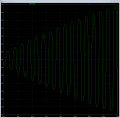
Now, using a 1kHz Vpp=0.1V input, using an Ideal NPN transistor, the result is the following:
4) Transient No Distortion Design.png
5) Transient No Distortion.png

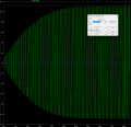
Using an Non Ideal NPN (BC238) transistor, the result is the following:
2) Transient Distortion.png
3) Transient Distortion.png


Clearly, the system is unstable!


Why is that? Have I used the wrong model? I just found it on the internet. Even for a non ideal transistor, this is weird, I've never seen this again.

BC238 Model (Source https://www.elelab.itu.edu.tr/belgeler/pspice/bc238.txt):
.MODEL BC238 NPN (
+IS =1.8E-14 ISE=5.0E-14 NF =.9955 NE =1.46 BF =400
+BR =35.5 IKF=.14 IKR=.03 ISC=1.72E-13 NC =1.27 NR =1.005 RB =.56 RE =.6
+RC =.25 VAF=80 VAR=12.5 CJE=13E-12 TF =.64E-9 CJC=4E-12 TR =50.72E-9
+VJC=.54 MJC=.33 )
In the attachments, you will also find three .rar files with the LTspice files for each of these simulations (DC Sweep, Transient BC238, and Transient NPN Ideal) for the last 2, I have named them Distortion and No Distortion.

Thanks!
 

Attachments

Jony130

Joined Feb 17, 2009
5,541
Clearly, the system is unstable!
No, this is not instability. Simply the BC238 has a much larger current (β) gain than the default model (this is not an ideal transistor).
Therefore, the circuit with BC238 is saturated that's all.

This is not the proper way of setting the DC quiescent current of a differential amplifier. The correct way is to connect R1 and R4 between the transistor bases and GND.
And we "set" the stage quiescent current by choosing a REE resistor only.
So, your example shows how not to bias the diff amplifier.
 

Thread Starter

babaliaris

Joined Nov 19, 2019
208
This is not the proper way of setting the DC quiescent current of a differential amplifier. The correct way is to connect R1 and R4 between the transistor bases and GND.
And we "set" the stage quiescent current by choosing a REE resistor only.
So, your example shows how not to bias the diff amplifier.
I don't know what to say. This is what they taught us in the Lab. We were actually using a potentiometer instead of R1, tunning it until V(C1) = V(C2).

No, this is not instability. Simply the BC238 has a much larger current (β) gain than the default model (this is not an ideal transistor).
Therefore, the circuit with BC238 is saturated that's all.
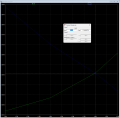
So why am I seeing the voltage gradually increasing in an exponential way? Is this going to be stabilized at some point in time? Do I need to do a transient with more periods in order to see that?

Oh, I see! It does go close to 15V, so it does saturate! This is weird... What can I do to fix that, without messing with REE or R4? In the lab I think it worked just fine, I just do not remember what the value of the potentiometer (R1) was.
Screenshot 2024-05-21 212152.png
 
Last edited:

Thread Starter

babaliaris

Joined Nov 19, 2019
208
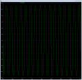
It seems to be doing the same. I used the 2N2222 with an Hfe of 100. From the output of the transient simulation, it seems like the gain is approximately 10V / 0.1V = 100. Is this possible?

Screenshot 2024-05-21 222400.png
 

Jony130

Joined Feb 17, 2009
5,541
It seems to be doing the same.
No. Now the DC operating point is fine. Transistors are not saturated for the DC.
From the output of the transient simulation, it seems like the gain is approximately 10V / 0.1V = 100. Is this possible?
The input signal is way too large in amplitude. Thus, the transistor for a positive peak will enter the saturation region.
So there is no point of calculating the gain if the amplitude of an output voltage is clipped.
 

Thread Starter

babaliaris

Joined Nov 19, 2019
208
Maybe because these labs haven't changed since the 90s? I believe this transistor and the μA741 OpAmp that we use are
pretty ancient.

Well, maybe they just teaching it wrong or they just simply don't care.

I'm already reading Sendra Smith's book and I'm planning on buying an Arbitrary Waveform and a Rigol Oscilloscope in the future and eventually mastering this knowledge myself.

I believe when it comes to Electronics we have the worst educators in my University.
 

Papabravo

Joined Feb 24, 2006
21,345
It is possible that both your institution and the available texts have failed you. It might just be a matter of consulting alternative sources to find the answers that you seek. It would not be the first time a student discovered the inadequacy of the initial resources. It looks like using a simulator to test the material has provided a valuable lesson. I wish it had been available when I first saw this material in 1967. Fortunately our text was first rate.
 

Thread Starter

babaliaris

Joined Nov 19, 2019
208
Is this design better? I thought of using two identical voltage dividers to make the common base mode voltage, independent from the transistor's base current (and probably from the HFe as well).

First I did a parameter sweep to set the dc point where the collector currents are approximately VCC/2 = 7.5V.
I found that R2=R4=R1=R3=10K. I picked 10K for R1, and R3 to have a relatively small starting current.

Param Sweep.png

Then I did an Operational Point Simulation to see if both transistors have the expected base currents, V(C) and that they are both not saturated:

Operational Point.png

Then, I did a transient for 2 periods. The amplification gives a gain of 25V/V 0.1v * 25 =2.5V, the signal is distorted though (for an input of 5mV << 26mV it is not, I tried it and it makes sense according to theory)...
It seems better than my Lab's notes, and since it (probably) works with this BC238 Bf=400, it proves that the voltage divider does indeed make it independent from the base currents:

Transient.png

Finally, I did an AC Analysis to see what is happening at 1kHz and the result is 47dB which gives a gain of 10^{47/20} =223.8V/V!!! What is wrong with that?

AC.png

Also, by the way, this C2 capacitor seems useless to me.
 

Attachments

Last edited:

Ian0

Joined Aug 7, 2020
10,293
When you have both negative and positive supplies, all you need to set the correct bias is a resistor to 0V (R2 and R4 in your diagram) if you are connecting a signal to that input.
If you don't need to connect a signal to the input, the transistor base can be directly connected to 0V.
 

Thread Starter

babaliaris

Joined Nov 19, 2019
208
When you have both negative and positive supplies, all you need to set the correct bias is a resistor to 0V (R2 and R4 in your diagram) if you are connecting a signal to that input.
If you don't need to connect a signal to the input, the transistor base can be directly connected to 0V.
I think I know what you're saying. Because I'm only giving one input to the first transistor Q1, the second Q2 does not do anything, so I could directly put its base to 0V and turn it off?

But If I give a differential input to both transistors with Q1 taking Vin and Q2 taking -Vin, then it make sense that both transistors are biased properly, so that the total differential amplifier will work in common mode. I think this example is better than my Lab's notes, and you can actually give some noise to the input to see if the amp successfully removes it, which is the best function of the differential amp (in common mode) in my opinion.
 

Ian0

Joined Aug 7, 2020
10,293
I think I know what you're saying. Because I'm only giving one input to the first transistor Q1, the second Q2 does not do anything, so I could directly put its base to 0V and turn it off?
Exactly.
But If I give a differential input to both transistors with Q1 taking Vin and Q2 taking -Vin, then it make sense that both transistors are biased properly, so that the total differential amplifier will work in common mode. I think this example is better than my Lab's notes, and you can actually give some noise to the input to see if the amp successfully removes it, which is the best function of the differential amp (in common mode) in my opinion.
Correct. A resistor to ground is the correct way.
The resistor can be Quite a high value, but if you get it too high there will be a voltage offset due to the voltage across the resistor resulting from the transistor base current.
V=IR/(2.Hfe)
Where I is the “tail” Current.
If you need a lot of usable common-mode input voltage, replace Ree by a constant current source, otherwise the tail current varies with the common mode voltage.

Someone has probably told you that when using op-amps, the resistances in both input circuits should be equal. That is where it comes from.
 

Thread Starter

babaliaris

Joined Nov 19, 2019
208
If you need a lot of usable common-mode input voltage, replace Ree by a constant current source, otherwise the tail current varies with the common mode voltage.
Yes, I know from theory that the best way is to use a mirror current for REE. Probably just for simplicity, we just used a resistor instead in the lab.

Someone has probably told you that when using op-amps, the resistances in both input circuits should be equal. That is where it comes from.
No, I knew that the inverting and the non-inverting inputs draw approximately zero current, but I didn't really know that both input resistances are equal.

Sedra/Smith explains how the Op-Amp is constructed in one of the last chapters, one day I will reach it and learn how it works :)
 

Jony130

Joined Feb 17, 2009
5,541
Is this design better?
Better, but you have chosen the DC op point wrongly.

In reality, all need is R2 and R4. R1 and R3 are unnecessary/redundant.
And change REE from 15kΩ to about (15V - 0.7V)/1.5mA = 10kΩ or 9.1kΩ
And you do not have to worry about BJT beta value.
Take a look at the simulation file that I have attached.

First I did a parameter sweep to set the dc point where the collector currents are approximately VCC/2 = 7.5V.
I found that R2=R4=R1=R3=10K. I picked 10K for R1, and R3 to have a relatively small starting current.
But your transition is saturated or is at the edge of saturation.
You have set VB1 to 7.5V (R1 = R2).
So the IEE = (7.5V - 0.7V + 15V)/15kΩ = 1.45mA so, Ic1 = Ic2 = IEE/2 = 0.725mA
And the voltage at the collector is:
Vc = 15V - 10kΩ*0.725mA = 7.75V

Vbc = 7.5V - 7.75V = -0.25V
and Vce = 7.75V - 6.8V = 0.95V

So we are very close to saturation. Almost at the edge of saturation.


Then, I did a transient for 2 periods. The amplification gives a gain of 25V/V 0.1v * 25 =2.5V, the signal is distorted though
Well, as I have shown you DC operating point is far from optimal. We have less than 1V for the "negative half cycle".
And you are still applying 0.1V, which is way too large for this amplifier.
The theoretical gain will be equal to about Rc/re = 10k/36Ω = 270 V/V. Therefore Vout = 0.1Vpeak *270 = 27Vpeak
However, we do not have room for such a large output amplitude.

Finally, I did an AC Analysis to see what is happening at 1kHz and the result is 47dB which gives a gain of 10^{47/20} =223.8V/V!!! What is wrong with that?
Nothing is wrong, AC analysis is showing idealized voltage gain, based on a small-signal analysis at the operation point.

Also, by the way, this C2 capacitor seems useless to me.
No, the C2 job is to short the Q2 base to GND for the AC signal. So 100nF is too low for F = 1KHz (Xc = 1.6k).
Without C2 the R3,R4 will affect the voltage gain slightly.
 

Attachments

Thread Starter

babaliaris

Joined Nov 19, 2019
208
Better, but you have chosen the DC op point wrongly.

In reality, all need is R2 and R4. R1 and R3 are unnecessary/redundant.
And change REE from 15kΩ to about (15V - 0.7V)/1.5mA = 10kΩ or 9.1kΩ
And you do not have to worry about BJT beta value.
Take a look at the simulation file that I have attached.


But your transition is saturated or is at the edge of saturation.
You have set VB1 to 7.5V (R1 = R2).
So the IEE = (7.5V - 0.7V + 15V)/15kΩ = 1.45mA so, Ic1 = Ic2 = IEE/2 = 0.725mA
And the voltage at the collector is:
Vc = 15V - 10kΩ*0.725mA = 7.75V

Vbc = 7.5V - 7.75V = -0.25V
and Vce = 7.75V - 6.8V = 0.95V

So we are very close to saturation. Almost at the edge of saturation.


Well, as I have shown you DC operating point is far from optimal. We have less than 1V for the "negative half cycle".
And you are still applying 0.1V, which is way too large for this amplifier.
The theoretical gain will be equal to about Rc/re = 10k/36Ω = 270 V/V. Therefore Vout = 0.1Vpeak *270 = 27Vpeak
However, we do not have room for such a large output amplitude.


Nothing is wrong, AC analysis is showing idealized voltage gain, based on a small-signal analysis at the operation point.


No, the C2 job is to short the Q2 base to GND for the AC signal. So 100nF is too low for F = 1KHz (Xc = 1.6k).
Without C2 the R3,R4 will affect the voltage gain slightly.
WoW, your explanations are perfect! I will check your circuit and I already know I need to learn more about diff amp biasing. I'm pretty sure I will see it in Sedra/Smith's book at some point, and it is going to be much better than my professors.

I noticed as well that I was at the edge of saturation and that really bothered me. Now I know for sure.

The AC Analysis was the most important question for me because I truly could not understand why I was getting that much of a gain. I thought that I should get the same as the 0.1v input, but I forgot that spice calculates the bode diagrams for small signals around the DC Bias point. Now it makes total sense!!

Thanks a lot!!!
 

Johnfoxwell

Joined May 23, 2021
17
It is possible that both your institution and the available texts have failed you. It might just be a matter of consulting alternative sources to find the answers that you seek. It would not be the first time a student discovered the inadequacy of the initial resources. It looks like using a simulator to test the material has provided a valuable lesson. I wish it had been available when I first saw this material in 1967. Fortunately our text was first rate.
 

Johnfoxwell

Joined May 23, 2021
17
I have spent a lot of time fixing problems with transistor circuits that simulated ok. In my day using the h-parameters to analyse the circuit was always the best solution. Having established the equations you can vary the parameters with ease. The world of simulation has let you down. Long live maths !!!!
 
Top