Current sink design to stress charging circuit (DAC,op-amp,mosfet)

Thread Starter

GoExtreme

Joined Mar 4, 2018
52
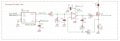
I'm trying to make a stress test circuit for charging circuit for 1 cell Lithium-ion batteries. See circuit drawing attached

Currently when charger is "on", connector get 4.35V from the charging circuit. I wan't to slowly increase the draw from low to high current.
Currently, even at low DAC output (0.02v), charger voltage is dropping to 0.80V with no current draw. Anything more then that drops it to 0v.

Is there a way to emulate the battery so I can pull current from charging circuit?
 

Attachments

Thread Starter

GoExtreme

Joined Mar 4, 2018
52
I don't understand.
How can the voltage drop if there's no current draw? :confused:
I don't understand either. Attaching graph of readings. If is set DAC to very low Its at around 0.8V, if I put little more its pulsing. Once I go over maybe 5% of DAC it just drop to 0v. Notice 0A current I don't get it.
SinkPulsing.jpg SinkPulsingMinDAC.jpg
 

danadak

Joined Mar 10, 2018
4,057
Your schematic looks nice ! Just 1 thing: if Rc is the load, Urc MAX = VCC - Uin. So the maximum voltage on Rc is limited by the voltage Uin.
Thats not quite correct, circuit controls current thru Rc, Vrcmax = Vin/Rr. Vin is
limited by OpAmp power supply common mode in limit for input pins.

Regards, Dana.
 
Last edited:

Joël Huser

Joined Jun 30, 2019
42
Thats not quite correct, circuit controls current thru Rc, Vrcmax = Vin/Rr. Vin is
limited by OpAmp power supply common mode in limit for input pins.

Regards, Dana.
Please Danadak, don't tell me that "Vrcmax = Vin/Rr".... the Ohm's law say better: "Irc = Vin/Rr"

BUT I claim again : Urcmax = VCC - Urr - Vcesat (transistor) =~ VCC - Urr = VCC - Uin.... so the max. voltage on Rc is limited by Uin. In other words, Urc can never reach VCC.

Could someone confirm danadak's comments or my comments ?

;-) Joël
 
Last edited:

danadak

Joined Mar 10, 2018
4,057
Boy did I screw that up, yes Vrc = Irc x Rc = (Vin / Rr) x Rc

Yes, Vrc is controlled by Vin.

And yes, when Vin drives NPN into saturation that will limit compliance
range of sink. Also overcoming Vbe turnon limits sink Vin to Iout transfer.


Regards, Dana.
 
Last edited:

danadak

Joined Mar 10, 2018
4,057
Here is a sim with bipolar. Whats driving the poor results is the
very high current that overcomes the ability of the OpAmp to supply
the base current for NPN.

upload_2019-7-5_7-13-52.png

I have been trying to get sim to run w/MOSFET, something is halting it
from producing meaningful results. However it is going to also have
limited results because you have to overcome the Vth of the MOSFET
before anything happens.

Regards, Dana.
 

Thread Starter

GoExtreme

Joined Mar 4, 2018
52
@danadak So do I need to remove resistors and capacitors from my design to make it work? Voltage coming in to mosfet is higher than 3.3v for op amp (4.35v).

currentSink.jpg
 

danadak

Joined Mar 10, 2018
4,057
No, leave Cs in, and the RC combination is for stability, I did not
evaluate the phase margin of the control loop to see if it is adequate.
You can do a quick bench eval by feeding OpAmp a pulse and look at
ringing on R55. 60 degrees or better good.

http://www.ti.com/lit/an/slva381b/slva381b.pdf


And keep your divider to meet CM input range of OpAmp. I just was
using a simplified model to do the sim.


Regards, Dana.
 
Last edited:

crutschow

Joined Mar 14, 2008
34,281
How can you implement a Mosfet ? Operationnal amplifier will adjust Vgs ? I know this schematic with NPN but not a N mos ;-) Joël
The circuit is a closed-loop with negative feedback so the op amp adjusts its output voltage to whatever is required to turn on the MOSFET, the same as it does for the NPN (the only difference is that the NPN requires about 0.7V to turn on whereas the MOSFET typically requires a few volts).
 

danadak

Joined Mar 10, 2018
4,057
Leave the footprints in for those components but that OpAmp is
comped for very heavy C load. Here is a sim I did, no evidence
of phase margin problems without the snubber as datasheet
discusses. Did this with 10 nS time step, more than enough for
this OpAmps bandwidth.

upload_2019-7-5_14-38-8.png

From datasheet -

upload_2019-7-5_14-40-0.png


The IRLZ44 has 1.7 nF input C, right around the graph loads shown above.

Try it w/o putting in components and look with a scope on output of OpAmp,
if it looks clean leave them out of design.

Note I also did SIM as small signal, no significant differences.


Regards, Dana.
 
Last edited:
Top