Facebook
 Google
 GitHub
 Linkedin
Hello,
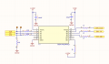
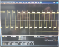
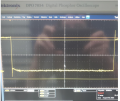
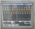
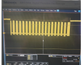
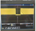
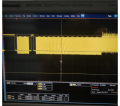
I am needing advice on the best practices of troubleshooting a design experiencing either EMI or ground connection issues causing interference with my data signal lines. I am attempting to communicate with an encoder using a simple bit banging method, using GPIO for the clock and data input signals. The peculiar problem I am having is that is seems to work correctly when I have a logic analyzer monitoring the CS, CLK, and DATA signals. Removing the probes of any of these results in corrupted data being read by the MCU. I have attached photos of the logic analyzer waveforms. I notice that there is still noise measured by the probe when all connections are attached, but it does not cause any issue in reading valid position data. The other graphs are when the CS, CLK, or DATA line probes are disconnected and the noise is very much an issue.
I have tried adding capacitors to ground on the lines but that was not improved performance. Any advice on how to proceed will be appreciated.
Attachments
-
 23.2 KB Views: 8
 -
 27 KB Views: 8
 -
 27.5 KB Views: 7
 -
 24.2 KB Views: 7