 Facebook
 Google
 GitHub
 Linkedin
Dear all,
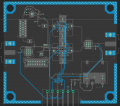
I have completed the designing of a 4-layer RF PCB and the manufacturer ask if it possible to balance the copper at the inner and outer layers.
The stack up is RF SIGNALS-GND-VCC-SIGNALS
This is my first PCB and I don't how to manipulate with copper balancing. Furthermore, I am not sure whether or not this extra copper is going to affect/degrade the performance of my RF PCB. Also, the extra copper shall be grounded or not?
Please find attached some screen shots (in single layer mode) of the layers.
Also, as you can notice I didn't apply vcc plane. Should I apply?
Thanks in advance
Attachments
-
 58.8 KB Views: 10
 -
 55.4 KB Views: 10
 -
 54.8 KB Views: 12
 -
 55.1 KB Views: 11


