controlled current source

Thread Starter

electronicsenjoyer089

Joined Feb 24, 2025
182
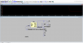
Hello all, i made a controlled current source with a mosfet N and an OP AMP, the thing i want to obtain is having fixed 150uA across the cap for certain amount of time, and after this the current has to drop to 0A.

Now i calculated in order to have 150uA during the positive cycle of the square wave ( So mosfet closes and the cap gets charged for the amount of time that the signal at "-" is HIGH ).

But i noticed that there is an issue, the current after 20us ( the time i decided for example ) doesnt go to 0, but it stays at 50uA or so, what i could do to fix such thing? can u please explain me what im doing wrong?

Thanks.
 

Attachments

Last edited:

dl324

Joined Mar 30, 2015
18,219
can u please explain me what im doing wrong?
Why do you have C1? With it, there is no DC path to ground for the opamp non-inverting input. With a 22k sense resistor, the 3.3V supply is too low. You might need a resistor on the output of the opamp. Many don't like driving a capacitive load and will oscillate.

Haven't looked up specs for the opamp or MOSFET...

BTW, that's a terrible symbol for the opamp.
 

Thread Starter

electronicsenjoyer089

Joined Feb 24, 2025
182
Why do you have C1? With it, there is no DC path to ground for the opamp non-inverting input. With a 22k sense resistor, the 3.3V supply is too low. You might need a resistor on the output of the opamp. Many don't like driving a capacitive load and will oscillate.

Haven't looked up specs for the opamp or MOSFET...

BTW, that's a terrible symbol for the opamp.
mosfet i looked at specs, for my requirements it has to have a time of switching below the 100us and it has to be able to carry atleast 250uA, im using C1 cus this schematic is just a part of a f-v converter, my idea is to give send pulses with different period, in order to charge the capacitor, then by doing a measurement of the cap i can understand whats the frequency of input signal, so for this stage i did like that.

Btw yeah i added a little resistor on the op amp output ( low resistor cus the gate behave like a capacitor, for now i tried with 100 ohm )
 
Once the C1 is charged to certain limit the constant current cannot be maintained anymore because of R1 drop or low gate voltage.

For imagine, the gate potential has to be at Vc1+Vr1+Vth.

Btw, the capacitor is usually placed into drain of transistor. This removes the low gate voltage problem.
 
Last edited:

Thread Starter

electronicsenjoyer089

Joined Feb 24, 2025
182
Once the C1 is charged to certain limit the constant current cannot be maintained anymore because of R1 drop or low gate voltage.

Btw, the capacitor is usually placed into drain of transistor. This removes the low gate voltage problem.
I dont wanna maintain it tho, i want that when the mosfet gate voltage is 0V then the current across the cap also has to be 0V
 

Thread Starter

electronicsenjoyer089

Joined Feb 24, 2025
182
Once the C1 is charged to certain limit the constant current cannot be maintained anymore because of R1 drop or low gate voltage.

For imagine, the gate potential has to be at Vc1+Vr1+Vth.

Btw, the capacitor is usually placed into drain of transistor. This removes the low gate voltage problem.
oh yeah so like that vgs is more precise and doesnt fluctuate, cus its tied to 0v the source, right.
 
You have swapped the +- inputs in op-amp since the negative feedback is needed, but your schematic wouldn’t work anyway.

It should be like this:
The 100/1k5 divider decreases the input 3v3 pulses about 15 times to get about 200mV as reference to +input. The current can be adjusted with R1.
IMG_2890.jpeg
If the C1 has to be placed on Gnd side you have to use a p-ch mosfet.
 

drjohsmith

Joined Dec 13, 2021
1,549
I wonder if a ne555 does what you want ?
its designed to charge a capacitor, and produce a pulse out , used to generate timing pukses
 

sparky 1

Joined Nov 3, 2018
1,218
A dual op amp can handle both the inverted and non-inverted forming a precision pulsed driver.
Identifying and measuring outputs in both the complimentary and inverted elements in the driver stage is helpful.
The correct specifications of a driver can then be applied to the storage and release of current in the power stage.
In figure 3 the circuit delivers 10mA and in figure 5 using a mosfet for more current. The skill reading, building, testing and analyzing.
AAC the land of broken toys.
AN-968: Current Sources Options and Circuits | Analog Devices
 
Last edited:

crutschow

Joined Mar 14, 2008
38,316
Your circuit does not generate a constant current, since the capacitor voltage affects the current reference voltage across R1 as it is charging.
Also just setting the input to 0V many not totally stop the charge due to various offsets.

Below is the LTspice sim of a high side constant-current circuit using an op amp and a P-MOSFET, to charge a grounded capacitor with the current determined by a TL431 voltage reference.

The current is started and stopped by Q1 which is not affected by offsets, and the capacitor reset to 0V by Q2.

Pot U2 adjusts the constant-current value.

1757012664017.png
 

Thread Starter

electronicsenjoyer089

Joined Feb 24, 2025
182
Your circuit does not generate a constant current, since the capacitor voltage affects the current reference voltage across R1 as it is charging.
Also just setting the input to 0V many not totally stop the charge due to various offsets.

Below is the LTspice sim of a high side constant-current circuit using an op amp and a P-MOSFET, to charge a grounded capacitor with the current determined by a TL431 voltage reference.

The current is started and stopped by Q1 which is not affected by offsets, and the capacitor reset to 0V by Q2.

Pot U2 adjusts the constant-current value.

View attachment 355376
This Is too complicated for me, what about the one the other guy Is showing?
 

crutschow

Joined Mar 14, 2008
38,316

crutschow

Joined Mar 14, 2008
38,316
If you are measuring the cap voltage with a multimeter, make note of the capacitor discharge and voltage drop due to the multimeters input resistance.
This can be significant for small capacitor values (below a µF).
 

sparky 1

Joined Nov 3, 2018
1,218
The possibility is in using the two 2N3904 to solve problems or just good use of switches.
Inside the op amp the matched pmos nmos arrangement and drive symmetry lends itself to better performance.

The experience level and help is much appreciated.
 
Top