Constructing an input sequence for an S'R' latch with NAND gates

Thread Starter

SumTingWong

Joined Jan 22, 2015
22
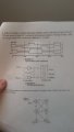
We are given the logic simulation of the latches behavior, the diagram, and the function table, and I'm not exactly sure what the input sequence is supposed to be, as wont the truth table show what the inputs are? It says to keep in mind that changes in state occur in response to 0 rather than 1. I can't find anything from googling 'input sequence,' maybe I'm over thinking this? The function table is here:

S' R' | Q Q'
0 1 | 1 0 set state
1 1 | 1 0
1 0 | 0 1 Reset state
1 1 | 0 1
0 0 | 1 1 Undefined
 

WBahn

Joined Mar 31, 2012
30,051
That table isn't a truth table -- look at what it says for input condition 11. The second line says that the output is 10 and the fourth line says that it is 01. What do you know about a NAND-based S'R' latch when both inputs are HI?

This appears to be a table of sequential inputs.
 

WBahn

Joined Mar 31, 2012
30,051
The S and R signals in Figure 5-5 are the input sequence (or at least AN input sequence).

I see what they are doing with the table in Figure 5-6 and it isn't the normal way of presenting the functionality of a circuit and I don't think it's a very good way to do it, either. The normal way is something like:

R'|S'|Q(n+1)|Q'(n+1)|comment
0|0|1|1| Disallowed state
0|1|0|1| Reset
1|0|1|0| Set
1|1|Q(n)|Q'(n)| Hold state
 
Top