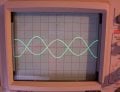
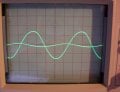
common emitter amp output distorted, can't figure out why, need help please

Audioguru

Joined Dec 20, 2007
11,248
Hmmm, and here I thought when a circuit hit the edge of its range it was clipping, which this circuit is doing. It is flattening out because it can go no further.
No.
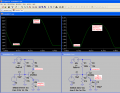
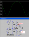
The output should go to +10.0V when the transistor is cutoff. But it goes up to only +8V because the compression distortion is very high.
When plenty of negative feedback is added then the output goes up to almost 10.0V and the compression distortion is much less.

Having Ce so high also means the input impedance of this circuit is extremely low, less than 10Ω.
No.
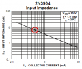
The input impedance is (hfe x re) which is 6.5k ohms and is also shown on the datasheet for the 2N3904 transistor.
 

Attachments

Wendy

Joined Mar 24, 2008
23,814
Except you are forgetting RL, it matters. If it weren't there the output could go all the way to the power supply (both AC and DC). Either way, the gain of this is way beyond 50 or so, since Volta is only getting less than half of the bottom of the sine wave.

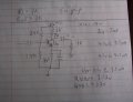
Again, you are leaving out Ce. If you bothered to read my math I calculated the input impedance at DC (I know it will be different at AC). The problem it, Ce is so large than it is effectively a few milliohms at AC. The emitter as far as AC is concerned is ground, leaving only the BE as the impedance for the AC signal.

Your values in the simulator are also way off.


Vcc = 14V
hfe = 170
R1 = 38KΩ
R2 = 12KΩ
R3 = 1KΩ
Re = 510Ω
RL = 1KΩ
C1 = 20µF
C2 = 8µF
Ce = 338µF (not sure where he got that value)
Freq = 100mv PP ???Hz

Your game is off today.
 
Last edited:

Audioguru

Joined Dec 20, 2007
11,248
Except you are forgetting RL, it matters
I added a load the same resistance as the collector resistor to my circuit and it simulates with the same severe compression distortion. The load simply reduces the voltage gain a little.

Again, you are leaving out Ce. If you bothered to read my math I calculated the input impedance at DC (I know it will be different at AC). The problem it, Ce is so large than it is effectively a few milliohms at AC. The emitter as far as AC is concerned is ground, leaving only the BE as the impedance for the AC signal.
I simulated my circuit with an emitter capacitor (no negative feedback) and without an emitter capacitor (plenty of negative feedback).
I showed the calculation for the input impedance with an emitter capacitor and also showed it from the datasheet.

The base-emitter diode has an impedance (52 ohms) that is 26 divided by the emitter current in mA but the input impedance of the transistor is beta TIMES the impedance of the diode. The AC beta (hfe) is 125. Therefore the input impedance is 52 x 125= 6.5k ohms.

Your values in the simulator are also way off.
The values do not matter. My transistor is biased preperly with its collector at almost half the supply voltage.
A transistor without any negative feedback produces severe distortion at high levels. Its base-emitter is current operated but we are feeding it a voltage signal instead. Its transconductance at low currents is very non-linear.
 

Attachments

Wendy

Joined Mar 24, 2008
23,814
Simulator values don't matter, guess that's why you don't show the same results as the OP. I predicted his actual P-P value within a couple 10ths of volts..

The OP also measured the hfe, a real value, not a theoretical one. Wanna guess what I used for my math?

AudioGuru said:
The base-emitter diode has an impedance (52 ohms) that is 26 divided by the emitter current in mA but the input impedance of the transistor is beta TIMES the impedance of the diode. The AC beta (hfe) is 125. Therefore the input impedance is 52 x 125= 6.5k ohms.
I can't argue that one way or another, but in the circuits I've built it usually is a lot lower than that. Lets just say I'm dubious at this point.

About the simulator values you say don't matter, the OP has a specific goal. I think he's going to have to tweak R3 downward to meet that goal (5V P-P), since RL is a hard given. Ce also has to be there, but I think it would be beneficial if it were a lot smaller, starting 1µF or smaller.

Simulators are good, but they don't teach the math behind the results. He needs to learn the math.
 

Wendy

Joined Mar 24, 2008
23,814
First time I've seen some take pride in an amateurish job... :D

I'm seeing some definite phase shift besides 180° in the Oscope.
 

hobbyist

Joined Aug 10, 2008
892
Sorry I wasn't trying to be prideful about it.
The person asked for help in understanding it.

I was just trying to help at an amature level.

I deleted the post.

Sorry if it came out the wrong way...
 

Wendy

Joined Mar 24, 2008
23,814
What! No sense of humor! Leave the post by all means, the more the merrier. If the ideas work, and Volta understands your explanations better than ours, the thread is a success.

I really was kidding you know, I thought the laughing emoticon would show that. I thought your solution was pretty good.

For the record, Hobbyist dropped Re down to what, 320Ω? He then adjusted the bias accordingly.
 

hobbyist

Joined Aug 10, 2008
892
What! No sense of humor! Leave the post by all means, the more the merrier. If the ideas work, and Volta understands your explanations better than ours, the thread is a success.

I really was kidding you know, I thought the laughing emoticon would show that. I thought your solution was pretty good.

For the record, Hobbyist dropped Re down to what, 320Ω? He then adjusted the bias accordingly.

Hi Bill,

I was definately overreacting,
I appreciate your reply back to straighten things out.

After I logged out I felt like a kid picking up his toys, and leaving the sandbox

I want to try to help the new people have a basic understanding of how these circuits can be designed to a working (half decent) condition just so they don't get discouraged. And give up trying all together.

Thanks again for taking the time to reply back.

I'll post it over again..
 

hobbyist

Joined Aug 10, 2008
892
Everyone is giving the PROFESSIONAL way of doing this.
I can only offer a Hobbyist way of going about this problem.
I used 14 volts as you chose for VCC.
steps:
1.) VCQ= 7v....... (1/2 VCC)
2.) ICQ = 7mA.
3.) Choose to make VCE to be 1v. so as to not saturate the transistor, during positive input.
4.) Now when positive signal comes in, Q1 will conduct enough current to drop its collector voltage VC, from 7vdc to 4.5vdc. in order to cause the voltage across RL to go from 0vdc. to -2.5vdc. due to capacitor coupling.
So when VCQ drops to 4.5vdc, that means (14v - 4.5v) will be across RC.
therefor the transitor must conduct (9.5v / 1k ohms) = 9.5mA. in order to put a -2.5v. signal across the Rload resitor.
5.) solving for RE. recalling VCE to be 1v. then volt across RE will be (VC - VCE) = (4.5v - 1v.) = 3.5v for VRE.
Now RE is solved by talking the new signal collector current into this voltage.
(3.5v. / 9.5mA) =~ 360 ohms.
Now under NO signal conditions VRE will be 360 ohms times ICQ= (360 * 7mA) = 2.52v.
6.) VRB then is 2.52v. + Vbe = 3.22v.
7.) Beta min =30 so IBQ = (7mA / 30) =233uA.
8.) base to ground (bleed off) resistor, = ~ {(VRB / IBQ) / 2} This equation works only for Beta min. (otherwise use 10*IBQ)
9.) solve for the supply base resitor the usual way.

100_1706.JPG

This is the the Vout of around 2.5v. pk. with a 2v pk. input.
Very little gain. due to RC // RL / RE (500 / 360) = Av.

100_1705.JPG

However by choosing a capacitor CE to be around 10 times less the RE at desired frequency, brought the gain up by reducing the input signal, and still achieving the 2.5v pk across the load.

100_1707.JPG
 
Last edited:

Audioguru

Joined Dec 20, 2007
11,248
Count Volta built the circuit then asked, "Why is the output so badly distorted and is "only" 4.4V p-p instead of 5V p-p?"

I simulated a transistor and showed exactly the same results.
I explained that the transistor needs a current signal input to be linear, as shown on his curve-tracer. I explained that with a voltage signal input then the base-emitter of a transistor is very non-linear without a lot of negative feedback.
I showed much lower distortion (and a higher output swing) when there is a lot of negative feedback.

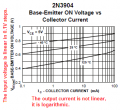
Here is the base-emitter voltage vs collector current of a 2N3904 transistor from its datasheet. Notice that the base-emitter input voltage is in linear 0.1V steps but its collector current steps are logarithmic.
Starting with a base-emitter voltage of 0.6V then the collector current is 0.1mA.
Step the base-emitter voltage up 0.1V to 0.7V and the collector current increases to 4mA. 40 times higher.

Again step up the input voltage 0.1V to 0.8V and the collector current increases to only 100mA. 25 times higher, not 40 times.

See the non-linearity? At low currents when the transistor is almost cutoff, changing the base-emitter voltage 0.1V results in a very small change in the collector current and therefore also results in a very small change in the collector voltage. It is severe compression of the positive-going part of the waveform which is distortion.
 

Attachments

Wendy

Joined Mar 24, 2008
23,814
I worked the math and explained why 4.4V PP. Electronics is about math, not just charts. The OP is a student, he needs the math tools to calculate it.

At this point we are waiting for the OP so he can ask questions.
 

Audioguru

Joined Dec 20, 2007
11,248
I worked the math and explained why 4.4V PP. Electronics is about math, not just charts.
Guess what, Bill.
I don't agree with you, the datasheets don't agree with you, my simulations don't agree with you and you also do not agree with yourself!
You calculated an output of only 3.46V, not 4.4V.

You assumed that the 3 capacitors have no reactance because maybe the frequency is high. But we don't know what is the frequency.
 

Thread Starter

count_volta

Joined Feb 4, 2009
435
LOL what a war I started. Might as well be the AC/DC wars of Tesla and Edison.

First of all my input frequency is 1khz.

I read what you guys said and I think you are both right to an extent.

Bill, isn't the purpose of CE to make the emitter ground to the ac signal? Then wouldn't we want a large capacitor to have a small impedance to short circuit Re?

This is how I got the capacitance values. They gave this to us in the lab report.

You may use the following formulae to calculate the bypass (CE) and coupling (CC1, CC2) capacitors to ensure a flat frequency response down to fLOW = 100Hz:

CE > 1/(wLOW *re)
CC2 > 10 / [wLOW (Rout + RL)]
CC1 > 10 / (wLOW *Rin)
where re is the emitter dynamic resistance given by re = VT / IEQ and VT is the thermal voltage.


I thought about it over and over and I don't get why it would be distorted. Everything seems right. The operating point gives plenty of room for a 5V PP swing for the ac output. I think the filter capacitors make sure that the transistor doesn't leave the active region by keeping the dc bias steady and keeping me at the operating point.


There is a trend I noticed, the output signal looks better and better as I decrease the input ac signal. The problem is 50mv Peak is as low as the function generator can go. If I go any higher it looks even more distorted. Can this be a clue as to what is going on?
 

Thread Starter

count_volta

Joined Feb 4, 2009
435
Count Volta built the circuit then asked, "Why is the output so badly distorted and is "only" 4.4V p-p instead of 5V p-p?"

I simulated a transistor and showed exactly the same results.
I explained that the transistor needs a current signal input to be linear, as shown on his curve-tracer. I explained that with a voltage signal input then the base-emitter of a transistor is very non-linear without a lot of negative feedback.
I showed much lower distortion (and a higher output swing) when there is a lot of negative feedback.

Here is the base-emitter voltage vs collector current of a 2N3904 transistor from its datasheet. Notice that the base-emitter input voltage is in linear 0.1V steps but its collector current steps are logarithmic.
Starting with a base-emitter voltage of 0.6V then the collector current is 0.1mA.
Step the base-emitter voltage up 0.1V to 0.7V and the collector current increases to 4mA. 40 times higher.

Again step up the input voltage 0.1V to 0.8V and the collector current increases to only 100mA. 25 times higher, not 40 times.

See the non-linearity? At low currents when the transistor is almost cutoff, changing the base-emitter voltage 0.1V results in a very small change in the collector current and therefore also results in a very small change in the collector voltage. It is severe compression of the positive-going part of the waveform which is distortion.
Yea thanks!! I'm glad you understand what I'm asking. That does sound like a realistic reason for the distortion, but how does it explain my observation that decreasing the input ac signal makes the waveform look better while increasing it, makes it look worse?

If I increase the input voltage, then doesn't the input current also go up, and as you say the distortion is caused by small ac current.

Maybe there is something I don't understand. Can you explain please.
 
Last edited:

Audioguru

Joined Dec 20, 2007
11,248
isn't the purpose of CE to make the emitter ground to the ac signal? Then wouldn't we want a large capacitor to have a small impedance to short circuit Re?
Of course. Then the voltage gain and distortion are very high.

I thought about it over and over and I don't get why it would be distorted. Everything seems right. The operating point gives plenty of room for a 5V PP swing for the ac output. I think the filter capacitors make sure that the transistor doesn't leave the active region by keeping the dc bias steady and keeping me at the operating point.

There is a trend I noticed, the output signal looks better and better as I decrease the input ac signal. The problem is 50mv Peak is as low as the function generator can go. If I go any higher it looks even more distorted. Can this be a clue as to what is going on?
Yes. You are feeding the transistor a voltage signal but your curve-tracer shows a current signal input. The current input is linear (low distortion) but the base-emitter of a transistor is non-linear (distortion) to voltage inputs. The higher the input swing then the higher is the distortion. With low input voltage swings then the distortion is not too bad because the input voltage does not go very low where the distortion is.

Weren't you taught that the internal emitter resistance, Re is "26 divided by the emitter current in mA"?
 

Thread Starter

count_volta

Joined Feb 4, 2009
435
Of course. Then the voltage gain and distortion are very high.
How exactly does shorting out Re to the ac signal do this? Don't you want to short out Re so that the ac signal does not disturb Ve and thus Vbe and thus keep the transistor at the operating point? Thats why you do this I thought.


Yes. You are feeding the transistor a voltage signal but your curve-tracer shows a current signal input. The current input is linear (low distortion) but the base-emitter of a transistor is non-linear (distortion) to voltage inputs. The higher the input swing then the higher is the distortion. With low input voltage swings then the distortion is not too bad because the input voltage does not go very low where the distortion is.
Hmm I need to think about this. Here is my schematic again.


I know the signal is a voltage but all voltages cause current. So the input voltage causes a proportional current that looks the same as the voltage but is divided by the resistors. So doesn't the transistor actually amplify that current? That is ib(t) which was caused by Vbe(t)?

I wish there was a way to see exactly whats going on here.

Weren't you taught that the internal emitter resistance, Re is "26 divided by the emitter current in mA"?
We were taught by Sedra and Smith book that Re = Vt/ie where Vt = 25mv (thermal voltage). Might you be referring to the same thing?
 

kingdano

Joined Apr 14, 2010
377
just going to post that this thread is great for someone who is lacking in analog electronics "chops" - and is a good reminder that math matters in electronics.

carry on brainiacs!
:D
 

R!f@@

Joined Apr 2, 2009
10,007
is the OP simulation a software ckt or an actual practical application.
if later the case then anyone ever thought of the ESR of the caps he is using
 

Thread Starter

count_volta

Joined Feb 4, 2009
435
What is an OP? Is that me? LOL.

I actually built the thing, not simulated it. What I showed you is a screenshot from an actual oscilloscope.

Anyway, once again I say thank you to the people who made the AAC ebook. I read the chapter on transistor biasing and it was all there the whole time. In all honesty Sedra and Smith spend waaaaay too much time on complicated math and not enough time explaining concepts. Their section on the emitter follower is horrible from the conceptual point of view.

The AAC section is crystal clear to me. Thanks guys, you just got me out of depression. Reading Sedra and Smith makes me feel like an idiot half the time. Oh just take the quadruple integral of such and such and you understand how it works right? :rolleyes:

I understand what Ce is for now. But there is a small typo in the ebook. Here. http://www.allaboutcircuits.com/vol_3/chpt_4/10.html

Bypass Capacitor for RE section.

It says
The solution for AC signal amplifiers is to bypass the emitter resistor with a capacitor. This restores the AC gain since the resistor is a short for AC signals. The DC emitter current still experiences degeneration in the emitter resistor, thus, stabilizing the DC current.
It should say

The solution for AC signal amplifiers is to bypass the emitter resistor with a capacitor. This restores the AC gain since the capacitor is a short for AC signals. The DC emitter current still experiences degeneration in the emitter resistor, thus, stabilizing the DC current.
 

bertus

Joined Apr 5, 2008
23,005
Hello,

The OP is used here for the "Original Poster", the one who started the thread.
You can aslo see TS for "Topic Starter" or "Thread Starter".

Bertus
 
Top