Class D amp -my working prototype

Thread Starter

RmACK

Joined Nov 23, 2007
54
A member asked me to share some info on my class D amp project.
I have been working on it for some time time now & am currently at the point where I have a working prototype.

Circuit Details:
I use 2 opamps configured as a schmitt trigger & integrator to create a triangle waveform. This is compared to my audio signal using a quad comparator. The comparator drives two high & low side drivers which in turn drive the mosfets. Thus I have a full bridge. Dead time is inserted using RCD networks on the inputs of the mosfet drivers. This allowed me to adjust the (very small) dead time. I did this as I was concerned that the dead time provided by many IR driver ICs would be too large for the high frequency operation I was aiming for of 650kHz. When loaded I can't get it linear and symmetrical above 250kHz so have changed the design to include a buffer.

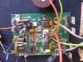
The circuit has been deliberately built using through hole components. The only surface mount parts are the two inductors in the output filter.

Upcoming tasks for me to do
-Measure the minimum dead time needed to avoid shoot through and compare it to the range of driver ICs available with dead time controls to see if it is feasible to change driver ICs, creating a simpler, more accurate & elegant dead time control.
-See how fast I can switch with improved pcb layout over the 1st revision board (the 100pF integrator cap was accidentally placed far from the integrator opamp)
-Reduce the quiescent current from 79mA @ 14V to <50mA.
-Build a final prototype
-Build a (already designed) speaker protection circuit for switch on
-Write up the entire project to share via my website (and on the forum)f

Attached are my schematics for all who are interested, feel free to comment. Note that this is a fully operational amplifier, not a conceptual one. Unfortunately the schematics have not yet been tidied after much tweaking & updating.

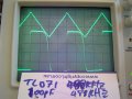
The scope photo shows my triangle wave working at nearly 0.5MHz.
I will try upload photos of the constructed circuit soon but my digital camera is stuffed so I'll have to find another way....
 

Attachments

Wendy

Joined Mar 24, 2008
23,415
Have you ever researched M type filters? In this case a M type low pass filter, they have really sharp knees in their curves which might be useful.
 

SgtWookie

Joined Jul 17, 2007
22,230
Not bad, but...
In your 1st schematic, you have overlapping values (upper left quadrant) hard to tread.
In your 2nd schematic, you have lots of "flying leads" near right side. As to where those might go, I haven't a clue - nor will most of our other readers.

Good start, needs work though.
 

Thread Starter

RmACK

Joined Nov 23, 2007
54
@Bill_Marsden:
Never heard of an M type lpf, will investigate. The main problem I have is trying to design a filter that has good rejection of the switching signal, but not attenuating at 20kHz by more than 3dB. That's ok except with such a low impedance load, the filter tends to suck quite a lot of current at the switch frequency, passing energy back & forth from the filter to the power supply, which I'd rather reduce.

@SgtWookie
With regards to the messy diagram, as mentioned, I have made modifications to the design after building it in response to issues that I had and have updated these changes into the schematic (to keep track) incrementally. These were painfully done from my very slow pc in the shed over remote desktop. I'll tidy it up of course but haven't done so yet, just very busy with several other persuits at the moment... The bits of wire you refer to go nowhere. They are legacy wires from when there were snubbers that were tested and found to be doing very little and from the switching waveforms don't appear necessary. Only labelled ports VCC, GND, Fet1, Fet2, Fet3, and Fet 4 go between the schematics. I'll upload the schematics again when I have tidied them but I am very busy with other things at the moment so it may be weeks away.

Thanks for the feedback, let me know any other ideas anyone has. As you can tell the project is close to completion (I can switch it on & listen to music!!) and I will present a proper description of how it works complete with photos & tidy schematics on my website some time this year.

Keep those filter ideas coming! Any ideas for how to improve damping factor? Don't want to suck too much current from the supply at switching frequency through the filter if possible. I already had to split my inductance in two to make it symmetrical for emi reasons -the non inductor speaker lead was radiating noise and ran close to a phone line, bringing down our ADSL internet at switch on and seriously decreasing the noise margin during operation!
 

Wendy

Joined Mar 24, 2008
23,415
Wikipedia article here.

Basic schematic...


This filter seems perfect for your application, the resonance frequency would notch your PWM carrier, and also has the effect of sharpening up the knee of the curve considerably.

I've tuned the bandpass version of these, and they are a stone female dog to tune. I suspect this one is going to be a lot simplier though, resonance is the key. The trade off is rejection ratio is less than a normal low pass might have.
 
Last edited:

Thread Starter

RmACK

Joined Nov 23, 2007
54
Thanks Bill :), I'll definitely try some simulations when I next get a chance, probably next weekend. I'll let you know how I get on.
 

Thread Starter

RmACK

Joined Nov 23, 2007
54
Have just measured the dead time that I am using. Depending whether you take into account the rise & fall times, 50 and 150nS. The fastest adjustable dead-time that I can find in an IR mosfet driver is 400nS so that means that I cannot improve over my current dead time arrangement. Thus, on to looking at those type M filters, then etching a new board & building before ordering a whole lot of boards from China.
 

Thread Starter

RmACK

Joined Nov 23, 2007
54
Thanks guys, this is such a helpful community! That's a great pdf, most was pretty familiar stuff, but it did offer a few interesting tips.

I had a go at simulating some M derived filters, got some really nice results (attached) but on the real amp it only made it worse (drew a little bit more supply current about 10% more even with fairly small caps).

As this filter arrangement is so similar to my existing one (just added the 18nF caps) I have gone ahead & ordered 20 pcbs from ourpcb.com which will, due to the superior layout allow me to run the amp at much higher switching speeds in turn assisting my filter design adjustments.

I'll get those schematics neat & upload soon. I also dismantled my camera and got it to take pictures again temporarily so got some of the amp but since doing so the usb doesn't work. (Damn little flexible pcb & the dodgy little connectors Sony used on them) Time for a new camera I think, it is 5 years old....
 

Wendy

Joined Mar 24, 2008
23,415
Like I said, the bandpass were a pain to tune, so why should the low pass be different? Hope springs eternal though. The good news is, when they are tuned, m derived filters perform exactly as theory predicts, it's the tuning that is the trick.

The m Derived filters I worked with were RF jobs, so I had hoped they would be better at lower frequencies. Are you using the bandpass blocking variety?
 

Thread Starter

RmACK

Joined Nov 23, 2007
54
I'm using a shunt low pass half section.
I'll have a crack at tuning when the new boards have arrived & I have got my final switching frequency sorted. Thing is my caps are around the 18nF mark so a bit high to be able to just pick up cheap trimmer caps for example.

I'll probably buy a handful of caps & use a sort of binomial trial and error system to hopefully get it tuned. Will report back on how this goes. Boards should be about a week away.

Attached are filter schematic & response. Note I am measuring current through a resistive load on the red curve and supplied current from amp on the green as my goals are
1)not attenuate the audio, this is close, the -3dB is about 19kHz
2)minimise current draw/maximise filter impedance at switch frequency, my measured frequency currently is 248kHz.

Thanks for the continued contributions :)
 

Attachments

Thread Starter

RmACK

Joined Nov 23, 2007
54
At last, I have photos...

Attached is a photo of the entire amp, most of it is on the pcb (see 2nd photo) except for the filter (taped to piece of wood) and a preamp with a gain of 3 on veroboard. Yes there have been a lot of changes since the pcb was designed, hence the mess but with the high switching frequencies I was aiming for, it was never really going to be a a breadboardable project.

The new pcb incorporates all these changes. I had 20 boards arrive yesterday. See 3rd pic old pcb on left, new on right. Much more compact and includes preamp and output filter. Should have a tidy built up (hopefully) working well by the end of the weekend! Oh and also should hopefully have tidied schematics by then too.
 

Attachments

Top