Class AB Push Pull Amplifier Design

Thread Starter

new-circuit8

Joined Aug 15, 2019
9
Hi,
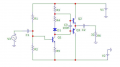
I am very new to electronics and have been given the attached AB amplifier circuit to analyse and select suitable components to suit the requirements.
Can anyone please give some tips where to start? (I don't want someone to do it for me - just need some advice to get going).
The requirements I have to meet (not included so I can do required calculations):
Output Power : ?? Watts
Output Load Resistance: ?? Ohms (This is R6 in the AB circuit)
Voltage Gain: ??
Low Frequency Roll-off Point: ??Hz
Rin: ?? Ohms
Cheers
 

Attachments

AnalogKid

Joined Aug 1, 2013
10,986
I don't understand the question.
Output Power : ?? Watts
Output Load Resistance: ?? Ohms (This is R6 in the AB circuit)
Voltage Gain: ??
Low Frequency Roll-off Point: ??Hz
Rin: ?? Ohms
These are the parameters *you* set in order to do the calculations that determine the component values. Without them you have no starting point.

ak
 

MrChips

Joined Oct 2, 2009
30,711
Welcome to AAC!

If you have questions related to school assignments then the thread goes in Homework Help.
The purpose of Homework Help is exactly that. We help you learn the material presented to you. You have to show your approach to the problem and then we can guide you along. We cannot supply you with the answer without your showing what you know.
 

Ylli

Joined Nov 13, 2015
1,086
You have the output load given, and I assume one of the specs you are given is minimum power output. Might want to start by determining appropriate V1 and V2 voltages.
 

Thread Starter

new-circuit8

Joined Aug 15, 2019
9
You have the output load given, and I assume one of the specs you are given is minimum power output. Might want to start by determining appropriate V1 and V2 voltages.
Thanks Yilli,
I have calculated the V1 and V2 voltages based off power output (1W) and load resistance (10 ohms) = +/-4.472v and Vo = 3.16v. This also lead to determining IL (IR6) = 3.16/10 = 316mA, which therefore determined the biasing current for Q2 = 3.16mA (assuming hFE: 100).
My voltage gain was nominated at 12dB which is equivalent to RC/RE = 4.
My Rin was specified to be >1000 Ohms and low frequency: 100Hz.
I'm not really sure where to start with sizing the resistors - I understand I need to set up the bias for Q1 but not entirely sure how to do.
Any guidance would be great!
 

Audioguru

Joined Dec 20, 2007
11,248
You calculated output RMS voltage and current. But the output must produce [b/peak[/b] voltage and current that is "the root of 2" (1.414 times) higher.
You did not calculate that the output transistors are emitter-followers that have a base-emitter voltage drop that might be 1V each at the fairly high peak current. Then I see that V1 and V2 should be at least + /- 5.5V.

ALL audio amplifiers have AC and DC negative feedback but yours doesn't.
 

Ylli

Joined Nov 13, 2015
1,086
To follow up on Audioguru's comments, Do you have any limitations as to the power supply voltages? Do you think it would be better to use a higher or lower power supply voltage?
 

Thread Starter

new-circuit8

Joined Aug 15, 2019
9
You calculated output RMS voltage and current. But the output must produce [b/peak[/b] voltage and current that is "the root of 2" (1.414 times) higher.
You did not calculate that the output transistors are emitter-followers that have a base-emitter voltage drop that might be 1V each at the fairly high peak current. Then I see that V1 and V2 should be at least + /- 5.5V.

ALL audio amplifiers have AC and DC negative feedback but yours doesn't.
Thanks for pointing that out @Audioguru! I'll re do my calcs accordingly! Yeah I have come to the realisation that this circuit is very uncommon as I have found no examples that are even remotely similar!
@Ylli, no I have no limitations on power supply voltages (will now be increasing based on Audioguru's RMS feedback).
@MrAI, no I have not determined them yet. I understand there needs to be about 1.2v difference between them though.
 

MrAl

Joined Jun 17, 2014
11,389
Thanks for pointing that out @Audioguru! I'll re do my calcs accordingly! Yeah I have come to the realisation that this circuit is very uncommon as I have found no examples that are even remotely similar!
@Ylli, no I have no limitations on power supply voltages (will now be increasing based on Audioguru's RMS feedback).
@MrAI, no I have not determined them yet. I understand there needs to be about 1.2v difference between them though.
Actually i meant the voltage right at the junction of the two emitters, not the two bases.
Can you figure out what it should be if the two power supplies are the same voltage (plus and minus that is) ?
Like say they are +10 and -10 volts.
 

Thread Starter

new-circuit8

Joined Aug 15, 2019
9
Wouldn't that be 4.472v RMS? (Sorry if that's an uneducated guess).
I think I'm getting closer but am still having difficulty determining R1 and R2 (Have been working on the circuit right to left based on the specs I received).
 

MrAl

Joined Jun 17, 2014
11,389
Well the first thing you should know is that if you want to get equal plus and minus swing at the output (to make full use of both power supplies) what should the output quiescent voltage be?
Say again we have +10 and -10 voltage supplies.
You want equal swing on the output to go as close to the rails as you can.
 

Thread Starter

new-circuit8

Joined Aug 15, 2019
9
Well the first thing you should know is that if you want to get equal plus and minus swing at the output (to make full use of both power supplies) what should the output quiescent voltage be?
Say again we have +10 and -10 voltage supplies.
You want equal swing on the output to go as close to the rails as you can.
That should be 0v?
 

MrAl

Joined Jun 17, 2014
11,389
Hello again,

Just in case you got a little lost here, we were working backwards too and now we have to calculate the base voltages of the two output transistors. In these circuits we usually start by assuming that the base emitter voltage drops are 0.7 volts and so the base voltages should be easy to calculate, and also assume that the transistor gains are all 100.
Next we will look at what kind of gain we need from the first transistor (the second two dont provide any gain so we have to get all the gain from the first transistor). After that we will look at how to optimize resistors R2 and R4 for quiescent operating current and voltage. In the end we can set the output voltage to zero (as you knew) and the emitter to emitter current to whatever we want it to be in order to reduce crossover distortion.
This is actually a good exercise in discovering the interplay between components in a multi component circuit like this.
 

Thread Starter

new-circuit8

Joined Aug 15, 2019
9
Thanks MrAI! I have made a lot of progress with the problem, calculating the required resistor values based off the voltage drops required to get to the 0v and the transistor base current. I am now at the stage of determining what size capacitors to use. I have my input resistance calculated (R1 // R2 // b x R5) but am not sure of my output? Is it just R6? I am getting a distorted output when I try with a circuit simulator.
 

MrAl

Joined Jun 17, 2014
11,389
Thanks MrAI! I have made a lot of progress with the problem, calculating the required resistor values based off the voltage drops required to get to the 0v and the transistor base current. I am now at the stage of determining what size capacitors to use. I have my input resistance calculated (R1 // R2 // b x R5) but am not sure of my output? Is it just R6? I am getting a distorted output when I try with a circuit simulator.
Well you have to show some work or at least the resistor values you have chosen.
That is the only way i can follow what you have done so far.
Also, how distorted is it. If it is very distorted then the resistor values may not be right yet.
And how much gain where you shooting for?
 

Thread Starter

new-circuit8

Joined Aug 15, 2019
9
MrAI,
Working done:
Peak R6 Voltage: sqr(2(10 x 1)) = 4.47v
Vcc = + / - 6.5v
Peak R6 Current: 4.47 / 10 = 447mA
Q2 Base I: 447mA / 100 = 4.47mA

R3 = (6.5 - [4.47 + 0.7]) / 4.47mA = 223
R3" = 223 // (R6 x 100) = 182

Av: 12dB
~ 10^12/20 = 4

R5: 182/4 = 45

Q1ci = (6.5 - 0.7) /223 = 26mA
Ve = 45 x 26mA = 1.17v
Vb = 1.17 + 0.7 = 1.87v

Q1bi = 26mA / 100 = 260uA
13 / 260uA = 50k

1.87 / 13 = 0.144

R2 = 0.144 x 50000 = 7200
R1 = 42000

Can you check and see if I'm going about it okay?
 

MrAl

Joined Jun 17, 2014
11,389
MrAI,
Working done:
Peak R6 Voltage: sqr(2(10 x 1)) = 4.47v
Vcc = + / - 6.5v
Peak R6 Current: 4.47 / 10 = 447mA
Q2 Base I: 447mA / 100 = 4.47mA

R3 = (6.5 - [4.47 + 0.7]) / 4.47mA = 223
R3" = 223 // (R6 x 100) = 182

Av: 12dB
~ 10^12/20 = 4

R5: 182/4 = 45

Q1ci = (6.5 - 0.7) /223 = 26mA
Ve = 45 x 26mA = 1.17v
Vb = 1.17 + 0.7 = 1.87v

Q1bi = 26mA / 100 = 260uA
13 / 260uA = 50k

1.87 / 13 = 0.144

R2 = 0.144 x 50000 = 7200
R1 = 42000

Can you check and see if I'm going about it okay?

Yes, but what is your output quiescent voltage and quiescent current in the emitter of Q2?
Also, is the gain you are going for going to be 4?
 
Top