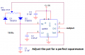
This simple circuit like others on the internet slowly destroys the BJT transistors because the maximum allowed reverse emitter-base voltage is exceeded (avalanche breakdown) each time a transistor turns off. The maximum allowed reverse emitter base voltage of most little transistors is only 5V or 6V but here they get almost 12V. A diode and resistor added to each transistor will fix it.
Google shows many circuits that have a multivibrator made with two Mosfets that produce a squarewave:
Is a square-wave out okay or would you prefer a sine-wave?
Of course that would require much more circuitry to generate a sine-wave modulated PMW signal to drive the transformer.
Is a square-wave out okay or would you prefer a sine-wave?
Of course that would require much more circuitry to generate a sine-wave modulated PMW signal to drive the transformer.
One way to get 120V peak out of that transformer is to drive the 12V side with a MOSFET bridge circuit from the 12V.
That will put ±12V across that 12V winding which will give ±120V from the 120V winding
You will need a proper bridge driver with non-overlapping signals to drive the bridge and avoid large current shoot-through during the switching time.
I have a circuit for that, if interested.
Below is the LTspice simulation of a non-overlapping clock driver with a complementary MOSFET bridge. The driver circuit uses three IC packages.
The NOR gates generate the non-overlapping function so that the top and bottom adjacent MOSFETs are never ON at the same time (the second and third magnified plots show this non-overlap for both rising and falling waveforms).
[Remember that the N-MOSFET gate (yellow) is high when ON, but the P-MOSFET gate (blue) is low when ON].
This prevents the high shoot-through current that would otherwise occur when the two transistors are momentarily on simultaneously during switching.
The red trace shows the ±12V waveform across the transformer winding (R_Trans).
Two CD4049 CMOS HEX inverter chips are used with three parallel outputs for each gate as a poor-man's push-pull circuit to drive the large MOSFET gate capacitance.
For driving a transformer, the input waveform should have an exact 50% duty-cycle.
That can be achieved by setting the 555 frequency to 100Hz and running that through a CD4013 flip-flop configured as a divide-by-2 toggle (/Q output to D input).
The 555 duty-cycle is thus not a factor, as the FF triggers on only one edge of the clock.
Note: Not shown, but required, are 100nF ceramic caps across each chip from their power pin to ground pin, as well a large (e.g. 100μF) cap from the bridge Vdd supply node to the bridge ground.
 Facebook
 Google
 GitHub
 Linkedin