 Facebook
 Google
 GitHub
 Linkedin
Hello all!
I am facing some challenges in designing a 4th order Butterworth LPF, implemented in MFB architecture. Since the LPF is of 4th order, it is divided into two stages cascaded together, each stage comprising of a second order Butterworth LPF. The schematic for each of the stage (2nd order Butterworth) and its transfer function is depicted in the following image.

The filter parameters can be mathematically represented through the following equations.

The optimised values for these filter characteristics have been documented in the following table.

For my application, I chose the gain of each stage to be 10x, and the cut-off frequency to be about 1KHz. The component values I am using for each of the stages are mentioned below.
Stage 1:
R1 (E) = 150
R2 (E) = 1500
R3 (E) = 5600
C1 (nF) = 4.7
C2 (nF) = 680
K = -10
FSF*fc = 971.3530391
FSF=1
fc (Hz) = 971.3530391
Q = 0.552479046
Stage 2:
R1 (E) = 680
R2 (E) = 6800
R3 (E) = 10000
C1 (nF) = 1
C2 (nF) = 330
K = -10
FSF*fc = 1062.4505
FSF=1
fc (Hz) = 1062.4505
Q = 1.282533103
The filter is working fine, but with three major problems.
1. The output response should show a gain of 10x, but it is neither showing any gain nor attenuation.
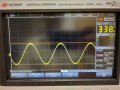
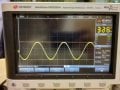
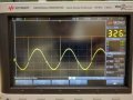
2. A glitch/spike is observed near each zero-crossing, its magnitude is very small at the output of the first stage but very large at the output of the second stage. Please find the snapshots of the input sine wave and outputs of both the stages in the attachments.
3. The system gives a cut-off frequency of about 160Hz (far less than the calculated value).
The magnitude of these glitches/spikes increase exponentially with frequency, and it is clearly evident especially in the output of the second stage.
As for the physical implementation of the system, it has been implemented on a PCB with SMD components, resistors having a tolerance of 1% and capacitors that of 5%.
I have tried different implementations by modifying the values of the discrete components as well as using a different Op-Amp IC, the results are more or less the same.
I would be really grateful if someone could point out what I am doing wrong.
Best regards,
Abbas.
I am facing some challenges in designing a 4th order Butterworth LPF, implemented in MFB architecture. Since the LPF is of 4th order, it is divided into two stages cascaded together, each stage comprising of a second order Butterworth LPF. The schematic for each of the stage (2nd order Butterworth) and its transfer function is depicted in the following image.
The filter parameters can be mathematically represented through the following equations.
The optimised values for these filter characteristics have been documented in the following table.
For my application, I chose the gain of each stage to be 10x, and the cut-off frequency to be about 1KHz. The component values I am using for each of the stages are mentioned below.
Stage 1:
R1 (E) = 150
R2 (E) = 1500
R3 (E) = 5600
C1 (nF) = 4.7
C2 (nF) = 680
K = -10
FSF*fc = 971.3530391
FSF=1
fc (Hz) = 971.3530391
Q = 0.552479046
Stage 2:
R1 (E) = 680
R2 (E) = 6800
R3 (E) = 10000
C1 (nF) = 1
C2 (nF) = 330
K = -10
FSF*fc = 1062.4505
FSF=1
fc (Hz) = 1062.4505
Q = 1.282533103
The filter is working fine, but with three major problems.
1. The output response should show a gain of 10x, but it is neither showing any gain nor attenuation.
2. A glitch/spike is observed near each zero-crossing, its magnitude is very small at the output of the first stage but very large at the output of the second stage. Please find the snapshots of the input sine wave and outputs of both the stages in the attachments.
3. The system gives a cut-off frequency of about 160Hz (far less than the calculated value).
The magnitude of these glitches/spikes increase exponentially with frequency, and it is clearly evident especially in the output of the second stage.
As for the physical implementation of the system, it has been implemented on a PCB with SMD components, resistors having a tolerance of 1% and capacitors that of 5%.
I have tried different implementations by modifying the values of the discrete components as well as using a different Op-Amp IC, the results are more or less the same.
I would be really grateful if someone could point out what I am doing wrong.
Best regards,
Abbas.
Attachments
-
 189.4 KB Views: 10
 -
 189.4 KB Views: 12
 -
 195.5 KB Views: 11


