Facebook
 Google
 GitHub
 Linkedin
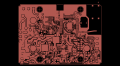
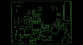
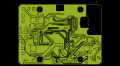
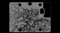
Hi all, in late 2018 I contracted a company to design me a board for my product. I paid them a large deposit and they told me I would have a sample unit in three weeks. Well after year I was told that the board will have to be redesigned and the new design will definitely work, when asked how long it will take for a new board I was told because of the virus they can’t commit. So they gave me the 4 layer board design and the BOM file. I had the boards made at great cost and gave them an empty board, the rest went from we are nearly there to only a voice mail. They did not give me the schematic is there a possibility to get that from the empty boards and BOM file? I hope I can find someone that can still use this board for my project.
Can one get schematic from a four layer board?
- Thread starter gombault
- Start date