Greetings,
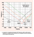
For some time I have been trying to understand the mechanism for bypass capacitors being used to eliminate power supply noise to galvanically connected devices. Each guide I have found describes what the the capacitor does and why it does but does not go into detail of how (the mathematics). Specifically, guides and datasheets say multiple bypass capacitors (of different values) placed in parallel will reject additional frequencies... how?
Consider the diagram (on a solderless breadboard):

My theory is this: Each capacitor combined with the parasitic inductance (and resistance?) of nearby components creates a band stop filter (concerning the device) at the resonance frequency; using multiple capacitors in parallel creates an array of band stop filters whos frequency bands overlap effectively creating a wider band stop filter. The incoming frequencies are shunted to ground due to a path of lesser resistance.
Any information is appreciated although I prefer mathematics over an intuitive response.
Regards,
Mark
For some time I have been trying to understand the mechanism for bypass capacitors being used to eliminate power supply noise to galvanically connected devices. Each guide I have found describes what the the capacitor does and why it does but does not go into detail of how (the mathematics). Specifically, guides and datasheets say multiple bypass capacitors (of different values) placed in parallel will reject additional frequencies... how?
Consider the diagram (on a solderless breadboard):

My theory is this: Each capacitor combined with the parasitic inductance (and resistance?) of nearby components creates a band stop filter (concerning the device) at the resonance frequency; using multiple capacitors in parallel creates an array of band stop filters whos frequency bands overlap effectively creating a wider band stop filter. The incoming frequencies are shunted to ground due to a path of lesser resistance.
Any information is appreciated although I prefer mathematics over an intuitive response.
Regards,
Mark

 Facebook
 Google
 GitHub
 Linkedin


