Facebook
 Google
 GitHub
 Linkedin
This exercise is confusing. They are talking about CE amplifier and voltage at the collector. But then they use T1 as an emitter follower and set DC voltage at the output to 1V. Strange.
And this is why the Author wrote vout = r_o2*ic?
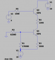
Re = (Vbb - Vbe - Vout)/Ie - Rb/(β1 + 1) ≈ (4V - 0.7V - 1V)/1mA - 10Ω = 2.3kΩ - 10Ω = 2.29kΩ
Another way of achieving a stiff voltage divider is to assume that R'B is 0.1*β*R'E.
Thus, the available voltage for T2 is 11V. T2 should be NPN type, of course, not PNP type, as was shown on the schematic.
The T2 will work as a current source only if T2 is in active region Vce > Vce(sat). So the Author decided to pic Vce2 in the middle of an available voltage 11V/2 = 5.5V.
And this is why we have R'E = 5.5V/1mA = 5.5kΩ
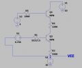
Notice that for the AC signal, Ib2 is 0A. No AC source signal is present at the T2 base, therefore ib2 * β2 must also be 0. Wich in the case of a current source means an open circuit.1. One thing that puzzles me in the textbook is that they get v_out = r_o2*ic?
And this is why the Author wrote vout = r_o2*ic?
Well, KVL. Vbb = Ie*Rb/(β1 + 1) + Vbe + Ie*RE + Vout. Thus, for Vout = 1V, Vbe = 0.7V and β1 = 100 we have2. How does the author get 2.29k for R_E?
Re = (Vbb - Vbe - Vout)/Ie - Rb/(β1 + 1) ≈ (4V - 0.7V - 1V)/1mA - 10Ω = 2.3kΩ - 10Ω = 2.29kΩ
It is another rule of thumb. In short, we want to have a stiff voltage divider (R1, R2). To achieve this, we usually choose a voltage divider current much larger than the base current, 10 x times usually.I DO understand why R'B is R1||R2, but I don't understand how why they are multiplying Beta,R'E, & 0.1 together. I especially don't understand what the 0.1 is where it came from, an why it's being used here.
Another way of achieving a stiff voltage divider is to assume that R'B is 0.1*β*R'E.
Yes.4. I See that the problem says the level shifter is connected to +/- 10V supplies. Is Vcc=10V and Vee=-10V?
We want to have Vout = +1V and this is the collector voltage of a current source (T2). The "bottom end" of a current source is connected to -10V (Vee).5. Sort of a followup to the last question, What is being averaged here exactly? I see 10V and 1V being averaged together does this have something to do with +/-10V supplies? And, if so, wouldn't we need to factor in more like 20V since there is a positive and negative rail of the same magnitude? Also, I presume the 1V comes form the 1V bias of the 2nd stage from the problem statement.
Thus, the available voltage for T2 is 11V. T2 should be NPN type, of course, not PNP type, as was shown on the schematic.
The T2 will work as a current source only if T2 is in active region Vce > Vce(sat). So the Author decided to pic Vce2 in the middle of an available voltage 11V/2 = 5.5V.
And this is why we have R'E = 5.5V/1mA = 5.5kΩ