 Facebook
 Google
 GitHub
 Linkedin
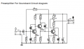
Please look at screenshot...
Interested in DC voltages..Before signal is applied.. 'Quiescent point"
correct?
Voltage at emitter of Q3 (V3)..Voltage at base of Q1(V1)
V3 = 80/47* V1 ? (yh?)
If so then can conclude, Voltage at collector of Q1 (Vx) :
Vx = V3 + 2Vbe
if correct, then assume Vbe = 0.65
then 47080*V1 = 47Vcc + 46906Vbe Checks out (about 100mv difference)
Is there an easier way to get the Quiescent?
Can't believe, designer went through this and we should calculate Quiescent before applying signal, no?
Btw, Please why all the non polarized(2 blacks) capacitors in schematic??
Thanks
Regards,
Mr Quiescent
Attachments
-
 57.6 KB Views: 16
 -
 349.3 KB Views: 15
 -
2.8 KB Views: 1


