 Facebook
 Google
 GitHub
 Linkedin
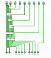
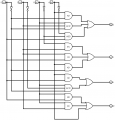
Hi, we are having a problem with making a binary to BCD converter. The first picture is the converter and the second picture is the add3 circuit. In total, we have used 42 ICs and a lot of wires. When we tested it, all the outputs are always logic 1. We are sure about the connections. We are guessing there is not enough supply voltage for the ICs. We are only using a 5V supply. What can we do to make this work. Thank you!!!!
Attachments
-
 9.7 KB Views: 20
 -
 9.7 KB Views: 19
 -
 9.8 KB Views: 20


