 Facebook
 Google
 GitHub
 Linkedin
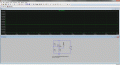
(In the circuit in the below schematic) there is a big discrepancy in voltage drop across the source resistor R3 according to simulation with Electronic Workbench (student edition) and what I measure at my actual, physical workbench. As this is such a simple circuit, I doubt that I have connected this up incorrectly at my bench.
So can anyone explain why simulated and actual voltages are so different?
I could comment some more at what I have been trying to do, but for now I'll leave it at that.
Thank you,
Pete

So can anyone explain why simulated and actual voltages are so different?
I could comment some more at what I have been trying to do, but for now I'll leave it at that.
Thank you,
Pete


")


