Astable multivibrator using CMOS gates - mathematical analysis

Thread Starter

xxxyyyba

Joined Aug 7, 2012
289
Here is my task.

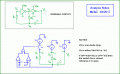
For astable multivibrator circuit find analytical expressions and sketch timing diagrams for voltages v1, v2, v3 and v4. It is known: R1, R2, C, Vdd, Vd (voltage drop on forward biased diodes) and Vthreshold (threshold voltage for CMOS circuit). CMOS inverters have protection diodes on input.


Here are my thoughts:

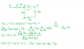
Let's sat at beginning that v2 = Vdd. It must be then v3 = 0. Equivalent circuit for this case is:


It is equivalent to this:


It is simple series RC circuit. It is easy to find solution for it (I wrote direct solution, I didn't show steps because it is not necessary).
Expression is valid till v1 goes to Vthreshold. It will occur at some T1. After solving equation v1(T=t1) = Vthreshold, we get T1=R2*C*ln(Vdd/(Vdd-Vthreshold)) = R2*C*ln2.

When v1 goes to Vthreshold, v2 will be low (= 0V) because v1 is high. v3 will be high in that case (= VDD). I stucked there. I don't know what to do next. Any idea?
 

MrChips

Joined Oct 2, 2009
30,802
Start with v1 = 0V, v2 = Vdd, v3 = 0V
C will charge through R2 from v2 as you have noted.
Vthreshold = Vdd/2 = v1
v2 = 0V, v3 = Vdd
this is going push v4 = v4 + Vdd
Take it from there.
 

Thread Starter

xxxyyyba

Joined Aug 7, 2012
289
It looks to me that, if v4 jumped from Vthreshold to Vthreshold + Vdd = Vdd/2 + Vdd = 3*Vdd/2, then v1 jumps also to same value.
 

MrChips

Joined Oct 2, 2009
30,802
v1 attempts to go to Vthreshold + Vdd but the input has protection diodes (D1 in this case).
Hence v1 does not go higher than Vdd + Vdiode.
 

Jony130

Joined Feb 17, 2009
5,488
Without any protection diodes, we can find time period quite easy.

The general formula for capacitor charging/discharging phase looks like this:

\( V_c(t) = V_{\infty} + \left ( V_o- V_{\infty} \right )e^{\frac{-t}{RC}} \)

Where \( V_o \) initial capacitor voltage value.

\( V_{\infty}\) is a steady state final value voltage.

And if we solve for \( t \) we will have

\(t = RC\,ln\left ( \frac{V_{\infty} - V_o}{V_{\infty} - V_c} \right )\)

So, for the case where (V3 = 0V and V2 = VDD)--> Vo = -0.5*VDD ; V∞ = Vdd and Vc = Vth = 0.5*VDD
We have
\(t = R_2 C\,ln\left ( \frac{V_{DD}- (-0.5V_{DD})}{V_{DD} - 0.5V_{DD}} \right )\)

\(t = R_2 C\,ln\left ( \frac{1.5V_{DD}}{ 0.5V_{DD}} \right ) = R_2 C\,ln\left ( 3\right ) \)

This is the half of the period, so the period is T = 2t = 2*R2*C*ln(3) ≈ 2.2*R2*C

But with the protection diodes, we have to include R1 current and R1 current flows only when V4 > VDD+Vd and for the negative V4 voltage (below 0V plus |Vd2|). The period at which R1 current is flowing is shown in red.

Ok. I will post my analysis procedure for this case.
I would like to see that.
 
Last edited:

MrAl

Joined Jun 17, 2014
11,472
Hi,

The main thing i think is that we have to first figure out what is controlling what,
then determine what voltage levels we have to look at, then what the times are due
to the way the cap charges and discharges.

First, V3 can be viewed as the driving force. That drives V4, which in turn drives
V1. V2 is driven by V1 alone, so once we know what V1 is doing we know what V2 is
doing, and that would wrap things up except for the fact that V1 is clamped to two
different voltage levels depending on the state of the circuit.
With V1 clamped that means we have to solve for the time up to the clamping action
and then the time after the clamping action. That will change the shape of V4.

For example, first as V3 goes high then V4 goes to a maximum for that state, and so
V1 goes max and is clamped, and the clamping action means that R1 is draining some
charge from the cap. After V4 drops somewhat the clamping action stops and we have
what i guess we would consider an open circuit for the first inverter input in this
kind of approximation, even though there is some input capacitance in real life.

So the main action is V3 changing, then R1 either in or out of the circuit.

This was after a quick inspection so feel free to disagree :)
 

MrChips

Joined Oct 2, 2009
30,802
The input resistance of a CMOS gate is very high. Hence R1 has little influence on the charge/discharge characteristics of C.
The frequency of oscillation is determined mainly on R2 and C.

On the discharge cycle when V2 = 0, C is initially charged to Vdd + ½Vdd and discharges to ½Vdd.

Hence V/V0 = ½Vdd/(Vdd + ½Vdd) = ⅓
ln(0.333) = -1.1 = -t/RC

t = 1.1 x RC

where R = R2

You get the same result on the charge cycle.

Thus the total period is approx. 2.2 x RC.
 

Jony130

Joined Feb 17, 2009
5,488
. Hence R1 has little influence on the charge/discharge characteristics of C
But what if someone decided to use R1 = 0.1R2 or even lower? And yes, I'm aware that rule of thumb says that R1 >> 10R2. But at the same time, R1 cannot be too large because R1 together with CMOS gate input capacitance (Cin) form a low pass filter. So, we need to keep R1*Cin << R2*C.

And I think that this is a job for TS to include the R1 effect on frequency. This is why he draw this protection diodes.
 

MrChips

Joined Oct 2, 2009
30,802
But what if someone decided to use R1 = 0.1R2 or even lower? And yes, I'm aware that rule of thumb says that R1 >> 10R2. But at the same time, R1 cannot be too large because R1 together with CMOS gate input capacitance (Cin) form a low pass filter. So, we need to keep R1*Cin << R2*C.

And I think that this is a job for TS to include the R1 effect on frequency. This is why he draw this protection diodes.
Because of the high input resistance on the CMOS gate, R1 can be as low as 0Ω.
As R1 approaches 1MΩ and higher, you start to notice an effect.
 

Jony130

Joined Feb 17, 2009
5,488
Because of the high input resistance on the CMOS gate, R1 can be as low as 0Ω.
I disagree. Ther will be a current flow through R1 resistor and via the protection diodes. And this current cannot be "large" because CMOS will lachup (CD400 series can by supply from 15V rail). This is why we put R1 in the first place also to improve the frequency stability.
 

MrChips

Joined Oct 2, 2009
30,802
I disagree. Ther will be a current flow through R1 resistor and via the protection diodes. And this current cannot be "large" because CMOS will lachup (CD400 series can by supply from 15V rail). This is why we put R1 in the first place also to improve the frequency stability.
Where is this "large" current coming from? It can only come from V2 and C.
CMOS latch-up is unlikely to occur. That is why the protection diodes are there in the first place.
I though we were looking for an analysis of the waveforms. That is what I have provided.
Your waveforms on post #3 say it all. I have provide the solution to the charge/discharge pulse widths
 

Thread Starter

xxxyyyba

Joined Aug 7, 2012
289
Let's continue analysis:
When v1 reaches threshold voltage Vthreshold, v2 falls to logical zero and v3 goes to logical one: v2 = 0, v3 = Vdd.
v4 = vc + Vdd = Vthreshold + Vdd = Vdd / 2 + Vdd = 3 * Vdd / 2 .
v1= Vthreshold + Vdd = 3 * Vdd /2, but because there are protection diodes on inputs, diode D1 start conducting, thus reducing v1 to Vdd + Vd.
Equivalent circuit for this case is:

cmos4.png

cmos5.png
We are interested in voltages vc(t) and v4(t). We can find Thevenin's equivalent circuit with respect to capacitor C:

cmos6.png

cmos7.png
cmos8.png
At some point in time (I will mark it as T2') diode D1 will stop conducting. When it happens, v1(t) will be slightly below Vdd + Vd. I will use approximation that v1(t) = Vdd + Vd (is it valid?).
Equivalent circuit in this situation will be:
cmos9.png

Last circuit is simple series RC circuit.

cmos10.png
 

Attachments

Last edited:

MrAl

Joined Jun 17, 2014
11,472
Hi again xxxyyy, Jony, MrChips,

I drew up this circuit earlier today but fell asleep before i could post it :)


xxxyyy:
I did not go over your work yet but i think you have the right idea. See attachment. Keep in mind though that there will be hysteresis too in addition to the threshold voltage VTH.

Jony:
I agree.

MrChips:
I believe you should take another look. See attachment which explains the situation better by removing the diodes from the circuit completely and replacing them with a simple logic circuit.
Note that when the switch is closed, R1 goes into effect, and that can happen in two different cases.
 

Attachments

Last edited:

MrAl

Joined Jun 17, 2014
11,472
Hello again,

Here are two equations i got so far which show the behavior of V4 when the output transitions from Vdd to 0v you can use for comparison:

[1]
(e^(-t/(C*R2)-t/(C*R1))*(R2*VTL+R1*VTL-Vdd*R2+Vd*R2-2*Vdd*R1))/(R2+R1)+(Vdd*R1-Vd*R2)/(R2+R1)

[2]
Vdd-Vdd*e^(-t/(C*R2))-Vd*e^(-t/(C*R2))

For the purpose of obtaining the time when V4 is less than 0 (just for curiosity):
Eq1 is valid for the period where V4<-Vd
Eq2 is valid for the period where -Vd<=V4<=0

and for the purpose of obtaining the entire low output period:
Eq1 is valid for the period where V4<-Vd as before,
Eq2 is valid for the period where -Vd<=V4<=VTH
where VTH is the CMOS input high threshold voltage trip point.

The choice of which inequalities to use and where (either less than or less than or equal to) is somewhat arbitrary here.

Note Eq1 is also dependent on R1 (which alters the timing), while Eq2 is not. The equivalent time constant is Rp*C where Rp is the parallel combination of R1 and R2. This makes that exponent -t/(Rp*C) of course.

The solutions check out within reasonable accuracy using a graphical technique for comparison to the calculations (about 3 digits) when using values R1=1k, R2=10k, C=100uf, VTH=3v, VTL=2v, Vdd=5v, Vd=0.6v. For example 0.1585 seconds calculated for the period where V4<-0.6 versus 0.160 seconds measured graphically.

VTH is the CMOS input high threshold voltage, VTL is the CMOS input low threshold voltage, Vd is the diode voltage that is assumed to be that value when forward biased and open circuit when the voltage is below that value, so it is an ideal switching diode.
I made R1 much lower than R2 to exaggerate the effect it has on the pulse times. In real life if this value was high it would have a much less effect.

Things that had to be considered for this output state:
1. The lower diode conducts for only part of the time after which the circuit reverts to a diodeless circuit.
2. The CMOS input threshold voltage hysteresis (1v used here).
3. Va was -Vd for this mode (see circuit in previous post).
4. The capacitor initial voltage for any mode after a transition is never zero. For this transition mode it is VTL-Vdd (left side is negative).
 
Last edited:

Thread Starter

xxxyyyba

Joined Aug 7, 2012
289
Just to say that I completed this task. After situation in post #15, v1 goes to -VD, v2=VDD and v3=0. By using same approach as before, I found relevant expressions for all voltages and I sketched other half of voltage waveforms (first half is in my previous post, post #16). I think that we did great job :) There is no analysis procedure for this circuit on web (at least I didn't find). There is only final result for period of oscillations.
 

MrAl

Joined Jun 17, 2014
11,472
Just to say that I completed this task. After situation in post #15, v1 goes to -VD, v2=VDD and v3=0. By using same approach as before, I found relevant expressions for all voltages and I sketched other half of voltage waveforms (first half is in my previous post, post #16). I think that we did great job :) There is no analysis procedure for this circuit on web (at least I didn't find). There is only final result for period of oscillations.
Hi,

So what did you get then? Also, did you determine if the output is a 50 percent duty cycle or something else?

I handled it as a three source circuit (with a switch) where we just had to determine what sources were doing what and then do the analysis. Of course we immediately have V2=Vdd-V3 so that simplifies it right off and once we declare V3 as the circuit excitation we always know what V2 is.

If you post some numerical results we can compare notes there too.

This was an interesting circuit to do. I am not sure if i had seen this circuit before or not because there are so many CMOS oscillator circuits out there.
 
Top