are logic gates abstract entities or physical?

Thread Starter

PG1995

Joined Apr 15, 2011
832
Hi

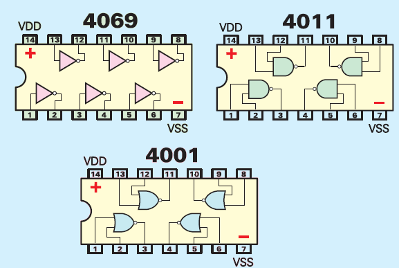
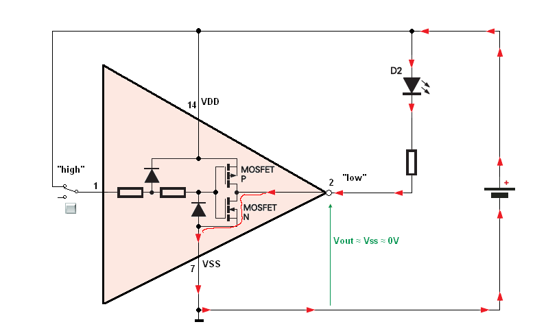
Would you please tell me if logic gates are abstract entities or real physical ones? How do they look? How are they made? I mean what electronics components, e.g diode, transistors, they contain inside them? Please help me with it.

Regards
PG

PS: Could you please link me to some picture which shows a 'physical' gate? I have googled but came across only circuit symbols for the gates.
 
Last edited:

thatoneguy

Joined Feb 19, 2009
6,359
The gates are an abstract representation, having a truth table showing what the output would be for the set of inputs.

There are many ways gates are built, and the7400 series has seen most of them in the line. ECL (Emitter Coupled Logic), DTL (Diode Transistor Logic), TTL (Transistor-Transistor Logic), CMOS (4000 series of Logic), etc.

The internal construction is usually several individual transistors, resistors, and/or diodes constructed to produce the Truth table in the shortest time possible. ECL is very fast, but takes a lot of current to function.

CMOS doesn't take much current (Relative to TTL), and isn't ultra-fast, but is a good trade off.

The outputs, or "fan out" (how many IC inputs one output can drive) is sometimes a critical need, so sometimes a different class of logic will be used for that purpose.

Other designs have outputs that are totem pole and "open collector", if you look in the e-book, Vol IV DIGITAL at the top of the screen, it will cover most all of this.
 

Thread Starter

PG1995

Joined Apr 15, 2011
832
Thank you very much, thatoneguy.

I think these main logic gates are building blocks which are used to make other things such as ROM just like transistors and other components are used to make amplifiers etc.

1: Does the designation "CMOS" in 'CMOS NAND gate' reflects the technology used to create the NAND gate? FET and BJT are both transistors but they have been manufactured using different technologies. By the way, I think the term "CMOS" also has something to do with digital camera because mostly cameras specify whether they use CMOS or CCD sensor.

2: Do the logic gates always use two inputs and one output. In the linked diagram you can see all the gates use no more than two inputs and just one output.

3: What is etymological background of term "truth table"? The table uses two kinds of values where "1" is called 'true' value and "0" false. So, it could be as valid to be called 'falsity' table as is 'truth' table.

Please help me with the queries above. Many thanks.

Regards
PG
 

monster_catfish

Joined Mar 17, 2011
116
Sweeping away a few cobwebs from the dusty recesses of my cranium, here are a few hazy recollections.

CMOS does refer to the substrate used to manufacture various semiconductors that are characterized by low power consumption, but high susceptibility to static electrical charge damage, and, if my memory serves me right, CMOS stands for Complimentary Metal Oxide Semiconductor

Logic gates do exist with multiple inputs, though each gate does have just one output, which, in some instances such as in sequential logic flip-flops may be fed back as an input line.

I can only guess at the reason for the semantics behind the name truth table. Suffice to say, a logic 1 state is denoted as a dc voltage of between 3 to 5volts dc, depending on the chip family, while a logic "0" is universally taken as zero volts, or circuit ground.
 

davebee

Joined Oct 22, 2008
540
Here are two physical gates, an AND gate and an OR gate.

The AND gate opens only if all padlocks have been opened, so its truth table is A AND B AND C AND ...

The OR gate opens if any padlock is opened, so its truth table is A OR B OR C OR ...
 

Attachments

MrChips

Joined Oct 2, 2009
30,712
Here are two physical gates, an AND gate and an OR gate.

The AND gate opens only if all padlocks have been opened, so its truth table is A AND B AND C AND ...

The OR gate opens if any padlock is opened, so its truth table is A OR B OR C OR ...
Neato! I will use this in my logic class.
 

colinb

Joined Jun 15, 2011
351
Here are two physical gates, an AND gate and an OR gate.

The AND gate opens only if all padlocks have been opened, so its truth table is A AND B AND C AND ...

The OR gate opens if any padlock is opened, so its truth table is A OR B OR C OR ...
Neato! I will use this in my logic class.
Just be careful not to get the students confused with the ambiguous usage of open and closed. For electrical circuits, open means no current may flow, while for fluid systems and these padlocks, open means current may flow (or the gate is free to move).

The terms open/closed are mainly confusing when you have a complex system with electronic control and many electrically actuated valves.
 

Jony130

Joined Feb 17, 2009
5,487
Q1
All the gate need external power supply. But sometimes (most of the time) we don't draw external power supply for the gate in the diagram.
But we all know that external power supply is necessary.
So if you buy the gate "chip" you need to connect external power supply to pins Vdd and Vee

Here you have some examples

bramkanot0.1_3099.jpg

http://forum.allaboutcircuits.com/showthread.php?t=40357&highlight=CMOS

Q2
Two arrows means the BJT with two emitters.


Q3
Yes, "Y" is the output terminal
 

Thread Starter

PG1995

Joined Apr 15, 2011
832
Thank you very much. I'm very much grateful for all the help. You have helped me with so many things.

Q1
All the gate need external power supply. But sometimes (most of the time) we don't draw external power supply for the gate in the diagram.
But we all know that external power supply is necessary.
So if you buy the gate "chip" you need to connect external power supply to pins Vdd and Vee
Please have a look here: http://img820.imageshack.us/img820/6783/jonydiagram1.png

Please have a look here: http://img4.imageshack.us/img4/7324/jonydiagram2.jpg

Q2
Two arrows means the BJT with two emitters.
Thank you for telling me this. I didn't know a transistor could have two emitters.
 

Wendy

Joined Mar 24, 2008
23,415
Actually it is two transistors with the bases and collectors connected, and the emitters left open.

You can do things with IC geometry that doesn't always translate well.

There have been similar discussions about this in the past. The diagram you have been looking is of the TTL (transistor transistor logic) family, but there are many familys of logic out there. DL (diode logic), DTL (diode transistor logic), RTL (resistor transistor logic) exist, and can be played with by making them with discrete parts, but have been abandoned as far as ICs are concerned because better has come out.

For the home experimenter CMOS is among the best characteristics, power supply range of +2 to +15 (or +20) volts, extremely high input impedance, extremely low output impedance (but very little drive, a negative), rail to rail logic levels, the logic goes to the power supply voltages, high noise immunity.

Transistor EXOR gate

logic families

Creating an XOR gate
 
Last edited:

Jony130

Joined Feb 17, 2009
5,487
Q1
Yes pins 8 and 9 are the inputs and pin 10 is the output.
But in this "chip" (IC) you have four separate (independent) NAND gates.
All this gate have a common power supply voltage rail.
And for CMOS logic we use VDD and VSS for describe external power supply terminals and Vcc/ Vee for bipolar circuit.
Look at diagrams that i post in this thread
http://forum.allaboutcircuits.com/showpost.php?p=258686&postcount=7

In this diagram
View attachment 34357
I show you how you can build a real circuit using CD40106 IC.
And this symbol in the middle inform as that this inverter IC has Schmitt trigger inputs.
And it is good practice to connect all your unused input pins to GND (Vss in this case) or to V+ (Vdd).
By doing so we prevent unused input from floating.
 

Thread Starter

PG1995

Joined Apr 15, 2011
832
Thank you, Bill, Bertus, Jony.

There have been similar discussions about this in the past. The diagram you have been looking is of the TTL (transistor transistor logic) family, but there are many familys of logic out there. DL (diode logic), DTL (diode transistor logic), RTL (resistor transistor logic) exist, and can be played with by making them with discrete parts, but have been abandoned as far as ICs are concerned because better has come out.
TTL, DTL, etc. are technologies to manufacture logic gates? That would mean I can get a TTL AND gate or DTL gate. Perhaps, both would have their own particular limitations.

For the home experimenter CMOS is among the best characteristics, power supply range of +2 to +15 (or +20) volts, extremely high input impedance, extremely low output impedance (but very little drive, a negative), rail to rail logic levels, the logic goes to the power supply voltages, high noise immunity.
I now roughly understand the term 'input impedance' which means very high input resistance and such an equipment would need very little power to operate. But what would the term 'output impedance' mean? Perhaps, it means that the equipment wastes very little power and most of the power generated is outputted.

What do you mean by "very little drive, a negative"? Please let me know if it's not difficult to understand.

Q1
Yes pins 8 and 9 are the inputs and pin 10 is the output.
But in this "chip" (IC) you have four separate (independent) NAND gates.
All this gate have a common power supply voltage rail.
And for CMOS logic we use VDD and VSS for describe external power supply terminals and Vcc/ Vee for bipolar circuit.
Don't you also use VDD and VSS for MOSFET circuits?

In this diagram
View attachment 34357
I show you how you can build a real circuit using CD40106 IC.
And this symbol in the middle inform as that this inverter IC has Schmitt trigger inputs.
And it is good practice to connect all your unused input pins to GND (Vss in this case) or to V+ (Vdd).
By doing so we prevent unused input from floating.
What are these Schmitt trigger inputs? And how do they differ from normal inputs?

I have heard the term "floating" in the context of electronics before. Perhaps, someone mentioned it while telling me how to operate a power supply, if I remember correctly. What does floating really mean? And what does really happen if it's floating?

In this diagram: http://img4.imageshack.us/img4/7324/jonydiagram2.jpg, Q4 is incomplete. I didn't realize it before. You have connected a LED followed by a resistor R2 to the output of a NOT gate (pin #12). I don't get it. In a gate the current flows from input to output. Therefore, how would the LED complete its circuit. Okay, after passing thru LED and R2 current enters the output but after that where does it go? I don't think LED should light up. Please help me with it.

Many thanks to you guys for all the help.

Best wishes
PG
 

Wendy

Joined Mar 24, 2008
23,415
You are correct as to what input impedance is. A typical CMOS gate measures several gig ohms on the input. Output impedance can be tricky, CMOS is relatively low output impedance, but there is an emphasis on relatively. With light loading they will go rail to rail on the power supplies and outputs, in other words when it is low out it will be very close to 0 volts, and when it is high it will be very close to Vcc volts. Load a CMOS gate even a little and it will not work well though.

CMOS gates also tend to use ½ Vcc as the transition point for logic levels, this is why they work so well on noise immunity. DTL and RTL both tend to try to treat anything over a volt as a 1, and even a small spike will be seen as a pulse.

Oh, and did I mention that if CMOS gates are not loaded they draw down in the nano-amp range? Many cases these gates don't even need on/off switches, they are so efficient. It is important to know and understand other logic families because you may need to fall back on them sometimes. I regularly use diode AND and OR gates because the parts count is so low and they are so convenient.

This is a purely personal preference, but I use Vcc for the plus side of the power supply, and ground (or GND) for the negative. Chip makers have their own standards, as do many manufacturers. You just have to pick it up as you go along.

There are logic families (ECL, emitter coupled logic) that use -2VDC as a logic low, and a -0.6V as a logic one. This is a major area where Vdd and Vss are used, but not the only ones.
 
Last edited:

Jony130

Joined Feb 17, 2009
5,487
Don't you also use VDD and VSS for MOSFET circuits?
Yes

What are these Schmitt trigger inputs? And how do they differ from normal inputs?
http://www.hobbyprojects.com/schmitt_trigger/schmitt_trigger_1.html


I have heard the term "floating" in the context of electronics before. Perhaps, someone mentioned it while telling me how to operate a power supply, if I remember correctly. What does floating really mean? And what does really happen if it's floating?
Well, floating refers to situation when a pin to an IC is left with no connection.


In this diagram: http://img4.imageshack.us/img4/7324/jonydiagram2.jpg, Q4 is incomplete. I didn't realize it before. You have connected a LED followed by a resistor R2 to the output of a NOT gate (pin #12). I don't get it. In a gate the current flows from input to output. Therefore, how would the LED complete its circuit. Okay, after passing thru LED and R2 current enters the output but after that where does it go? I don't think LED should light up. Please help me with it.
You can read here how gate work
http://www.allaboutcircuits.com/vol_4/chpt_3/1.html

And for example if we get inverter (NOT) gate and connect input node to positive terminal of a power supply.
So we have input at "high," or in a binary "1" state and the output is in "low" state or binary "0".


So output of a gate is sinking the current to provide a "0" or "low" state.
Vout is almost equal GND.
Ands as you can see the output current will flow for external power supply (pins 14 and 7)
 
Top