Facebook
 Google
 GitHub
 Linkedin
I have to understand the functioning of the boot strap capacitor, i followed the link Bootstrap it was clear till certain stage then ..

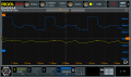
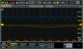
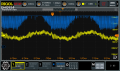
The charging part was clear when the lower Mosfet is ON the bootstrap capacitor charges as per VCC(1 - e^{-t/tau}) as it is PWM input, tau = Rboot * Cboot. Now the question is when the top Mosfet is ON there is a statement in the document in the link

Is the above statement wrong since the point Vs is directly connected to DC+ it can have voltage of VDC+ only.
I have verified another document TIBootstrap

The point HB should be VDC+ + VCboot (that is DC bus voltage + Voltage of the boot capacitor). There shall be internal connection between HB and HO, then only the HO the gate voltage will be greater than the source voltage which is HS and the Mosfet will be turned ON. Is my understanding correct?
The charging part was clear when the lower Mosfet is ON the bootstrap capacitor charges as per VCC(1 - e^{-t/tau}) as it is PWM input, tau = Rboot * Cboot. Now the question is when the top Mosfet is ON there is a statement in the document in the link
Is the above statement wrong since the point Vs is directly connected to DC+ it can have voltage of VDC+ only.
I have verified another document TIBootstrap
The point HB should be VDC+ + VCboot (that is DC bus voltage + Voltage of the boot capacitor). There shall be internal connection between HB and HO, then only the HO the gate voltage will be greater than the source voltage which is HS and the Mosfet will be turned ON. Is my understanding correct?