Almost-Fully digital High Power PSU, am I overlooking something?

Thread Starter

Lorenzo Di Mauro

Joined Oct 16, 2016
27
Hello guys, I have "designed" this theoretical circuit to convert any voltage up to 25 V to 12 V (And after that, 5 V & 3.3 V to make a full battery-powered ATX PSU)

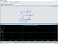
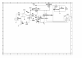
For a single PSU, this is the theoretical circuit. I do not use any sort of overshoot protection because the 500 KHz clock generator is a placeholder for a PIC16 MCU, and I was thinking on making a software-controlled overshoot protection by simply ramping up the PWM signal slowly via software to ensure there isn't a substantial Ramp up to 19+ Volt (way out of spec for ATX maximum 13V limit I'd say).

However I'm only a stupid student and I'm not sure this is the actual way to do this, the circuit is not that complex, however there are way too many components for just one rail, and I was wondering if any of you big guys have a suggestion to either:

* Reduce component size

* Avoid Inrush current to reach something on the line of 100+ A (To reduce trace width size), since my maximum current should be 10 to 15 A.

* Correctly calculate Inductor and Capacitor values

* Any issue I'm overlooking or straight up not noticing.

Any suggestion is appreciated, I want to make this a full blown ATX PSU (10 A for 3.3V, 5 V and 12V foe ULP PC) for a project I've been longing to do.
 

Attachments

Thread Starter

Lorenzo Di Mauro

Joined Oct 16, 2016
27
So, here's a better image where I did some refinements, made it look nicer and stuff like this.


Taking into account the Input Voltage to be between 24 and 18 V, I have simulated the correct PWM to be Between 65-45 (for Heavy-Light Load) and 75-55 (Same but for 18 V)

So I made the usual buck converter setup using an extremely low RDS(On) N Channel MOSFET (we are talking less than 1 mOhm "Low").

Inserted it together with a decently sized ideal inductor and oversized ideal capacitor and a 16 A temporary diode while waiting to make it synchronous with another AUIRFS8409.

The PWM is, as already said, generated by a PIC MCU via software, which has a feedback loop via The voltage output divider RDIV1-2 (Which converts a maximum of 15 volts to 5 theoretical volts - perfect for ADC Sampling), at a frequency between 750 KHz or 1 MHz.

The output of the MCU, being inherently not enough to drive anything useful, it sent to a High power Current amplifier which converts it to a respectable 22 V - 100 mA Output - Perfect to drive the low capacitance MOSFETS.

The output is then sent (and also inverted) to the two low-capacitance mosfets used to turn on and off the main Mosfet, ensure it doesn't fall into some sort of "unknown linear state" or simply gets turned on/off too slowly for my necessities.

What am I overlooking here, except lacking synchronous rectification and using uncorrectly sizes Inductors and Capacitors?

I noticed, running a simulation on Multisim, that the current taken by the MOSFET reaches levels of 100 A - 400 A, is this a simulation error or should I do something to prevent excessive input current? And if so, what is the best choice for this level of power?

Also, is the way I setup all these components wrong? Could I obtain similar results with lesser components?
 

ronv

Joined Nov 12, 2008
3,770
So, here's a better image where I did some refinements, made it look nicer and stuff like this.


Taking into account the Input Voltage to be between 24 and 18 V, I have simulated the correct PWM to be Between 65-45 (for Heavy-Light Load) and 75-55 (Same but for 18 V)

So I made the usual buck converter setup using an extremely low RDS(On) N Channel MOSFET (we are talking less than 1 mOhm "Low").

Inserted it together with a decently sized ideal inductor and oversized ideal capacitor and a 16 A temporary diode while waiting to make it synchronous with another AUIRFS8409.

The PWM is, as already said, generated by a PIC MCU via software, which has a feedback loop via The voltage output divider RDIV1-2 (Which converts a maximum of 15 volts to 5 theoretical volts - perfect for ADC Sampling), at a frequency between 750 KHz or 1 MHz.

The output of the MCU, being inherently not enough to drive anything useful, it sent to a High power Current amplifier which converts it to a respectable 22 V - 100 mA Output - Perfect to drive the low capacitance MOSFETS.

The output is then sent (and also inverted) to the two low-capacitance mosfets used to turn on and off the main Mosfet, ensure it doesn't fall into some sort of "unknown linear state" or simply gets turned on/off too slowly for my necessities.

What am I overlooking here, except lacking synchronous rectification and using uncorrectly sizes Inductors and Capacitors?

I noticed, running a simulation on Multisim, that the current taken by the MOSFET reaches levels of 100 A - 400 A, is this a simulation error or should I do something to prevent excessive input current? And if so, what is the best choice for this level of power?

Also, is the way I setup all these components wrong? Could I obtain similar results with lesser components?
Hi Lorenzo and welcome to AAC.
I see a couple of things to at least worry about from the hardware standpoint.
I think the gate to source voltage on the FETs is 20 volts. So in the case of 24 volts input it will be to much.
The 2 FETs that drive the big one will have some overlap where they are both on. This may be destructive.
With the large gate resistors in the drivers they will be to slow to run at 500KHz.
I think 24 volts is to high to run the high speed op amp.
You should be able to use a much smaller filter capacitor.
I would be concerned that the micro may be to slow to use to close the loop for voltage control. Think about an all hardware design.
 

Thread Starter

Lorenzo Di Mauro

Joined Oct 16, 2016
27
Hi Lorenzo and welcome to AAC.
I see a couple of things to at least worry about from the hardware standpoint.
I think the gate to source voltage on the FETs is 20 volts. So in the case of 24 volts input it will be to much.
The 2 FETs that drive the big one will have some overlap where they are both on. This may be destructive.
With the large gate resistors in the drivers they will be to slow to run at 500KHz.
I think 24 volts is to high to run the high speed op amp.
You should be able to use a much smaller filter capacitor.
I would be concerned that the micro may be to slow to use to close the loop for voltage control. Think about an all hardware design.
I mostly see what you mean. They are effectively going beyond reccomended values when they have 24+V

And I also thought about the overlapping issue, even though it shouldn't be a problem since the OFF Mosfet is supposed to turn ON slower than the ON mosfet does.

when simulating it, I get these values:


so i'm not sure if I should be concerned or not about that.

The simulation doesn't show any issue with the resistors limiting the switching capability of the MOSFET, i chose them for the exact purpose of having a low gate charge (and thus be able to turn off with smaller current values), even though I could also use a second OP Amp to drive both MOSFETS and negate the input of the first OP AMP on the second (thus creating an effective NOT Gate)

However, I don't understand what you mean by using a smaller filter capacitor (you mean I can get away with those massive 4000 uF? I thought so too)

And with the MCU being too slow "to use to close the loop for voltage control." what exactly do you mean by that? Do you think a 32 MHz MCU is not enough to drive a 500 KHz PWM input?

Anyway, thanks for your actual suggestions, I will look into either lowering the Input voltage or getting higher voltage components. Or a third unknown solution like using a 20V regulator to ensure everything works as expected (but I think it would be a bad idea).

I have thought of a full-hardware design, and the last time I tried, it was a failure, starting from the Oscillator to the error amplifier and comparator. That's why I thought about going full-digital: The MCU is easy to program, is (should be at least) plenty fast to drive such a low frequency signal, and it's efficient (well, more than the OP AMPS).
 

ronv

Joined Nov 12, 2008
3,770
I mostly see what you mean. They are effectively going beyond reccomended values when they have 24+V

And I also thought about the overlapping issue, even though it shouldn't be a problem since the OFF Mosfet is supposed to turn ON slower than the ON mosfet does.

when simulating it, I get these values:


so i'm not sure if I should be concerned or not about that.

The simulation doesn't show any issue with the resistors limiting the switching capability of the MOSFET, i chose them for the exact purpose of having a low gate charge (and thus be able to turn off with smaller current values), even though I could also use a second OP Amp to drive both MOSFETS and negate the input of the first OP AMP on the second (thus creating an effective NOT Gate)

However, I don't understand what you mean by using a smaller filter capacitor (you mean I can get away with those massive 4000 uF? I thought so too)

And with the MCU being too slow "to use to close the loop for voltage control." what exactly do you mean by that? Do you think a 32 MHz MCU is not enough to drive a 500 KHz PWM input?

Anyway, thanks for your actual suggestions, I will look into either lowering the Input voltage or getting higher voltage components. Or a third unknown solution like using a 20V regulator to ensure everything works as expected (but I think it would be a bad idea).

I have thought of a full-hardware design, and the last time I tried, it was a failure, starting from the Oscillator to the error amplifier and comparator. That's why I thought about going full-digital: The MCU is easy to program, is (should be at least) plenty fast to drive such a low frequency signal, and it's efficient (well, more than the OP AMPS).
Mmm, I missed the biggest problem. Q2 needs to be a P channel or you need to use a high side driver.
I think for a start try using an IR2184 driver. Then you have everything you need to drive both the pass transistor, but also the synchronous FET.
Maybe just something like a 7812 to produce the voltage for the gates.
 

Thread Starter

Lorenzo Di Mauro

Joined Oct 16, 2016
27
Mmm, I missed the biggest problem. Q2 needs to be a P channel or you need to use a high side driver.
I think for a start try using an IR2184 driver. Then you have everything you need to drive both the pass transistor, but also the synchronous FET.
Maybe just something like a 7812 to produce the voltage for the gates.
I could use a driver and I could use a 7812 as well, but why should I change Q2 (The Main transistor) to a P Channel? Isn't N Channel supposed to be better because of faster switching times and Lower RDS(On)?

I mean we're talking if I use a (for example) 6 mOhm P Mosfet at 20 Amps shouldn't the power dissipation go up to 2.4 W? Wouldn't it get HOT as in BURNING Hot?

I actually made calculations for a P Channel IPB80P03P4L-04, here are my findings:

TJ = 120 °C

RDS(On) (25 °C) = 3.7 mOhm
RDS(On) (25 °C) = 4.5 mOhm

RDS(ON)HOT = 3.7 * (1 + 0.005 * (120 - 20)) = 5.4575 mOhm Using Math.

PDSYNCHRONOUS RECTIFIER = [(21 * 21) * 5.4575] * [1 - (12/24)] = 1.20337875 W

PDRESISTIVE = [ILOAD² × RDS(ON)HOT] × (VOUT/VIN) = 1.20337875 W

PDSWITCHING = (CRSS × VIN² × fSW × ILOAD)/IGATE = (((65 * 10^-12) * (24^2) * (500 * 10^3) * 20))/1 = 0.3744 W

OJA = 62 °C / W

TJ(RISE) = PDDEVICE TOTAL × ΘJA = 97.8222825 °C

TAMBIENT = TJ(HOT) - TJ(RISE) = 22.1777175 °C

Wouldn't I still require some low form of active cooling to achieve this? Or should I go with parallel MOSFETs?

Also, being the MOSFET a low capacitance one, I should be safer with the gate drivers altogether, aren't I?

It clearly is the first time someone proposes me a P channel device, I'm not sure how to handle this.
 

ronv

Joined Nov 12, 2008
3,770
I could use a driver and I could use a 7812 as well, but why should I change Q2 (The Main transistor) to a P Channel? Isn't N Channel supposed to be better because of faster switching times and Lower RDS(On)?

I mean we're talking if I use a (for example) 6 mOhm P Mosfet at 20 Amps shouldn't the power dissipation go up to 2.4 W? Wouldn't it get HOT as in BURNING Hot?

I actually made calculations for a P Channel IPB80P03P4L-04, here are my findings:

TJ = 120 °C

RDS(On) (25 °C) = 3.7 mOhm
RDS(On) (25 °C) = 4.5 mOhm

RDS(ON)HOT = 3.7 * (1 + 0.005 * (120 - 20)) = 5.4575 mOhm Using Math.

PDSYNCHRONOUS RECTIFIER = [(21 * 21) * 5.4575] * [1 - (12/24)] = 1.20337875 W

PDRESISTIVE = [ILOAD² × RDS(ON)HOT] × (VOUT/VIN) = 1.20337875 W
No, you are correct. N channel is better, but to turn on the N channel the gate should be about 10 volts higher than the source. Since you want 20 volts on the source (FET on hard) you should have 30 volts on the gate. One way to fix that is to use a PFET so a negative voltage will turn it on. The other way is to use a bootstrap driver like the IR2184 that will raise the gate voltage. If your simulation will let you look at the power in the FET you will see it is very high.
I'll draw one up.

PDSWITCHING = (CRSS × VIN² × fSW × ILOAD)/IGATE = (((65 * 10^-12) * (24^2) * (500 * 10^3) * 20))/1 = 0.3744 W

OJA = 62 °C / W

TJ(RISE) = PDDEVICE TOTAL × ΘJA = 97.8222825 °C

TAMBIENT = TJ(HOT) - TJ(RISE) = 22.1777175 °C

Wouldn't I still require some low form of active cooling to achieve this? Or should I go with parallel MOSFETs?

Also, being the MOSFET a low capacitance one, I should be safer with the gate drivers altogether, aren't I?

It clearly is the first time someone proposes me a P channel device, I'm not sure how to handle this.
Edit: Don't know what happened to my typing..:D
Yes, NFET is better, but to turn it on all the way the gate needs to be 10 volts higher than the source. Since you don't have a 30 volt supply it will act like a source follower and get very hot.
The drive will give you the higher voltage. I'll draw one up.
 
Last edited:

Thread Starter

Lorenzo Di Mauro

Joined Oct 16, 2016
27
I'd rather not use a High side driver unless it really is cost effective compared to a handmade solution.

Is it really any better to use it at all?
 

ronv

Joined Nov 12, 2008
3,770
I'd rather not use a High side driver unless it really is cost effective compared to a handmade solution.

Is it really any better to use it at all?
I think the driver will be quite a bit cheaper than the FETs. It also has built in dead time so you don't have to worry about the FETs being on at the same time.
Attached is your driver. Notice the current during switching,
Also an example of the high side in an all hardware buck converter.
 

Attachments

Thread Starter

Lorenzo Di Mauro

Joined Oct 16, 2016
27
So, your suggestions opened a spark in my eyes, so I decided to go the "fuck it" way and went full digital / full integrated.

I created a 5 V rail for the 5VSB Using a TPS54531DDAR 5 A Buck converter

For the 12 V I went with a synchronous LM27222M MOSFET Driver which is also powered by the 5 A Buck Converter

For the MCU I went for a PIC12F1571 for it's low pin count (8), fast frequency (32 MHz) and ADC / PWM Capability, which will be used to drive the driver effectively, providing added security.

I went ahead and made both the schematic and the PCB, and I'd love to hear your suggestion about it:

http://www40.zippyshare.com/v/r56AFTRS/file.html
 
[


So, your suggestions opened a spark in my eyes, so I decided to go the "fuck it" way and went full digital / full integrated.

I created a 5 V rail for the 5VSB Using a TPS54531DDAR 5 A Buck converter

For the 12 V I went with a synchronous LM27222M MOSFET Driver which is also powered by the 5 A Buck Converter

For the MCU I went for a PIC12F1571 for it's low pin count (8), fast frequency (32 MHz) and ADC / PWM Capability, which will be used to drive the driver effectively, providing added security.

I went ahead and made both the schematic and the PCB, and I'd love to hear your suggestion about it:

http://www40.zippyshare.com/v/r56AFTRS/file.html
I attempted to open up your file, which prompted me to install some software called zippyshare, which it has all the look and feel of adware....thanks, but no thanks.

If you want to share an image, save it as .PNG, this provides very efficient compression. Best of all, it is transparent o Windows, Android and IOs programs, which will open it.
 

Thread Starter

Lorenzo Di Mauro

Joined Oct 16, 2016
27
? I usually use either zippyshare or mediafire for conversion, are you sure you were trying to download it correctly?

Either way, I'm more than happy to post PNGs here, so here they are:

SCHEMATIC:


TOP PCB:


BOTTOM PCB:


3D View:


I actually designed this solution to let me put a decently sized heatsink that attaches to both the Diode (TO-220AB) and the two MOSFETs (d2pack-7). I also made custom 2mm holes to let me directly test this circuit with a 6p test battery.
 

ronv

Joined Nov 12, 2008
3,770
? I usually use either zippyshare or mediafire for conversion, are you sure you were trying to download it correctly?

Either way, I'm more than happy to post PNGs here, so here they are:

SCHEMATIC:


TOP PCB:


BOTTOM PCB:


3D View:


I actually designed this solution to let me put a decently sized heatsink that attaches to both the Diode (TO-220AB) and the two MOSFETs (d2pack-7). I also made custom 2mm holes to let me directly test this circuit with a 6p test battery.
Unless you are changing to logic level FETs five volts is not enough to drive them.
I'm not sure what your plan is for the micro, but I found this write up. Is this what you have in mind?
http://ww1.microchip.com/downloads/en/AppNotes/00216a.pdf
 

Thread Starter

Lorenzo Di Mauro

Joined Oct 16, 2016
27
Unless you are changing to logic level FETs five volts is not enough to drive them.
I'm not sure what your plan is for the micro, but I found this write up. Is this what you have in mind?
http://ww1.microchip.com/downloads/en/AppNotes/00216a.pdf
As far as I understood the driver doesn't actually use VCC for driving the MOSFETs (which is absurd to me but the circuit is basicly copy-pasted form referente design with very little changes) so yeah... I guess it should work . it should also be a logic level mosfet since the treshold is in the 2 V range.

As for the site , I'll definitely look into it to discover new stuff, but I'm definitely not going to ditch this project to buy one of those ever.

The microcontroller is not a Real problem, I already know how to work with one of these. i'm using PWM rather than PSM
 

ronv

Joined Nov 12, 2008
3,770
As far as I understood the driver doesn't actually use VCC for driving the MOSFETs (which is absurd to me but the circuit is basicly copy-pasted form referente design with very little changes) so yeah... I guess it should work .
Actually it does use Vcc. When the lower transistor is on the capacitor gets charged thru the diode (missing in schematic) and the lower FET. This voltage then gets added to the source voltage when the top FET is told to turn on. You can Google bootstrap circuit to see more.
it should also be a logic level mosfet since the treshold is in the 2 V range.
I can't see a new part number in the latest schematic but the FET in the original is not a logic level. The threshold voltage in the spec is the voltage where the FET just barely turns on. To get the low Rds may take much more.
upload_2016-10-21_18-15-8.png

upload_2016-10-21_18-17-25.png

The microcontroller is not a Real problem, I already know how to work with one of these. i'm using PWM rather than PSM
I'm just worried that you are thinking of doing some processing to modify the pwm. There usually isn't enough time to do that.
Gotta watch those bicycles. :eek:
 

Attachments

Thread Starter

Lorenzo Di Mauro

Joined Oct 16, 2016
27
Actually it does use Vcc. When the lower transistor is on the capacitor gets charged thru the diode (missing in schematic) and the lower FET. This voltage then gets added to the source voltage when the top FET is told to turn on. You can Google bootstrap circuit to see more.
I can't see a new part number in the latest schematic but the FET in the original is not a logic level. The threshold voltage in the spec is the voltage where the FET just barely turns on. To get the low Rds may take much more.
View attachment 114032

View attachment 114033


I'm just worried that you are thinking of doing some processing to modify the pwm. There usually isn't enough time to do that.
Gotta watch those bicycles. :eek:
So, what do you suggest? Should I go for a different MOSFET altogether or check for a different solution?
 

ronv

Joined Nov 12, 2008
3,770
So, what do you suggest? Should I go for a different MOSFET altogether or check for a different solution?
Unless you are using the micro for something else I would drop the micro and just use a high speed comparator like shown in the simulation I posted. Then you could use a 12 volt regulator and a driver that works on 12 volts. This type is called a hysteretic buck converter.
 

Thread Starter

Lorenzo Di Mauro

Joined Oct 16, 2016
27
Unless you are using the micro for something else I would drop the micro and just use a high speed comparator like shown in the simulation I posted. Then you could use a 12 volt regulator and a driver that works on 12 volts. This type is called a hysteretic buck converter.
I am using the Micro basically only to control ALL PWM regulations to make things smaller. size is kind of a necessity to me and I should be able to control PWM quickly enough to change the D.C with my MCU.

I could also turn the +5V signal from the MCU to any voltage level using a high speed OP AMP. But I truly need to have it digital.

The reason I'm using a DIP PSU in the PCB Screen is to program it in a breadboard for easier programming
 
Top