Facebook
 Google
 GitHub
 Linkedin

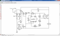
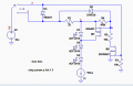
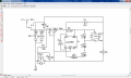
Yes, R2 is not needed.1. so it's ok to completely eliminate R2? can i make R4 a 5k resistor like R3 or make them both 10k? trying to minimize parts.
The value of R2 is not critical and 10kΩ will be fine.
Any transient to Z1 has to go through R2, thus it would take a large transient to damage Z1.2. transients will come from engine starters, pump motors, etc. with vicious load dumps. i don't know how big they are but these are what blew zeners before without TVS protection. what do you think?
But a TVS diode wouldn't hurt.
You need both zeners, since each MOSFET gate needs its own protection.3. i'm already using N mosfet for polarity protection on a different project. it's hooked up like i show in last schematic. it's working good so far. my question is - do i need both zeners or will Z1 protect Nfet gate from over voltage?
It holds the voltage to 12V only for Vgs of Q1.. i'm still confused on the effect Z1 will have on driver chip. if voltage supply is 24 volts, the driver chip compensates and used less current from supply. will Z1 always hold voltage at 12v regardless of input voltage? if so, don't think i like that.
It has no effect on any other voltage.
The dissipated power is I²R or .08 x .4² = 12.8mW.5. on resistance is 80mohm. .08ohm x .4a =.032w. is that right? here's the parts i picked.
N- http://www.mouser.com/ds/2/115/DMN6140L-709504.pdf 140mohm/2.3a
P- http://www.mouser.com/ds/2/115/DMP4065S-537770.pdf 80mohm/3.4a
seems both should be ok for 1amp. am i right?
Both of those appear to be more than adequate.