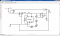
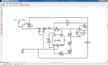
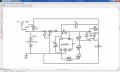
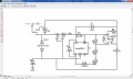
again, turning 1 LED off in string of 3 with 2 drivers?

Thread Starter

joewales44

Joined Oct 8, 2017
218
this time i don't need to dim, just turn off or on.
i can only use 1 switch.
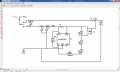
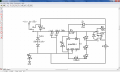
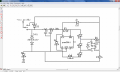
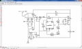
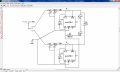
please tell me if this circuit will work.
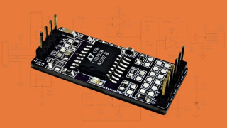
can the drivers share 1 inductor since only 1 driver is powered up at a time?
is the LX pin disconnected when the chip is not powered up?
if there is a better way, please let me know.
thanks
upload_2017-11-2_15-51-20.png
 

Thread Starter

joewales44

Joined Oct 8, 2017
218
FYI
built this circuit but it doesn't work right. current should be .348A.
the 2 LED side pulls .21A.
the 3 LED side pulls 1.5A.
so i guess there is some connection through the other chip even though it's not powered up?
guess i'll add another inductor and run separate circuits. i wonder if having grounds connected will still cause problems.
any idea what's going on here?
thanks
 
Last edited:

crutschow

Joined Mar 14, 2008
38,681
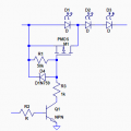
You don't need two drivers.
Just connect the three LEDs in series with one driver and use a high side P-MOSFET switch across the LED you want to turn off, as shown below.
When the MOSFET is off the LED lights.
When the MOSFET is on it carries the current and the LED is off.

D4 and R3 are needed to protect the MOSFET gate if the input voltage is greater than the maximum Vgs rating for the MOSFET.
upload_2017-11-10_10-26-13.png
 

Thread Starter

joewales44

Joined Oct 8, 2017
218
remember, i'm an electronics idiot.
1. i understand your design but doesn't that require a second switch to turn Q1 on or at least a 2 throw switch with a diode between throws?
this brings up something i've always wondered about.
2. can i use a N channel in the same way and turn it on with positive voltage from 1 side of 2 throw switch with a diode between throws?
3. to clarify my question, can either type mosfet, P or N, be used to complete a circuit whether on positive side or ground side? seems the gate voltage is only thing that would matter if the source and drain are just completing the circuit?
4. and does it matter which way the source and drain are oriented? i've seen them both ways in different circuits.
5. if the mosfet has any resistance at all, wouldn't the LED turn on a little?
would this work?
thanks
 
Last edited:

Thread Starter

joewales44

Joined Oct 8, 2017
218
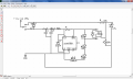
after more thought, what about this?
doesn't the gate need to be connected to ground through a resistor so it isn't floating when power is removed?
and i guess it does matter which way a mosfet is connected if it has internal diode?
will this work? are my resistor values ok?
thanks
upload_2017-11-10_16-57-8.png
 

crutschow

Joined Mar 14, 2008
38,681
what about this?
That's closer.
But the MOSFET won't fully turn off due to the two resistors.
Vgs must be near 0V to turn off the MOSFET (when the switch is in the up position).

And you are showing an N-MOSFET.
It needs a P-MOSFET with the source up.

The modification below should work:

upload_2017-11-10_14-6-50.png
 

Thread Starter

joewales44

Joined Oct 8, 2017
218
don't get me wrong, i'm asking, not telling.
why won't a npn work? it makes powering the gate a lot simpler to my weak mind.
 

crutschow

Joined Mar 14, 2008
38,681
don't get me wrong, i'm asking, not telling.
why won't a npn work? it makes powering the gate a lot simpler to my weak mind.
You mean an N-MOSFET?
NPNs are BJTs.

Actually it makes it very difficult.

To fully turn on, an N-MOSFET requires that the gate voltage be 10V more positive than than source voltage (for standard MOSFETs).
You can't achieve that in you circuit since the MOSFET source voltage is already near the plus supply voltage.

Conversely, to turn on, a P-MOSFET has to have the gate voltage 10V more negative than the source voltage (or the source voltage 10V more positive than the gate).
This is readily achieved in my circuit by grounding the gate, since the source is already at at least +11V.

Make sense?
 

Thread Starter

joewales44

Joined Oct 8, 2017
218
yes, makes perfect sense. i didn't know it had to have the 10 volt difference.
but i'm still confused about your diagram.
2. what is purpose of R3? i barely have enough voltage to run the LEDs without a resistor.
3. i don't understand your zener placement. i guess it only takes effect above 12volts? will it trick the driver chip? why does it connect before R3?
4. would this mosfet work? i'm only running 400mA. http://www.mouser.com/ds/2/115/DMP4065S-537770.pdf
why do they show negative amp rating?
5.when switch is up, i understand there would be only 1 volt on gate from the 50k and 5k divider. but when switch is down, it seems the gate would still be low. maybe if you show the switch or rest of the circuit i could understand.
thanks a million

upload_2017-11-10_20-32-36.png
 

crutschow

Joined Mar 14, 2008
38,681
Why is your circuit different from what I posted?
2. what is purpose of R3?
It is the unlabeled resistor (please label them) in you schematic between pins 4 and 5 of the 2861.
3. i don't understand your zener placement. i guess it only takes effect above 12volts? will it trick the driver chip? why does it connect before R3?
Yes, it limits the maximum Vgs to 12V.
Most MOSFETs have a Vgs limit of 15 to 20V.
It has no affect on the driver chip.
It's connected before R3 so the zener current won't affect the LED current.
4. would this mosfet work? i'm only running 400mA. http://www.mouser.com/ds/2/115/DMP4065S-537770.pdf
why do they show negative amp rating?
That MOSFET should work fine.
The drain current is negative because in normal operation the current direction is from source to drain.
5.when switch is up, i understand there would be only 1 volt on gate from the 50k and 5k divider. but when switch is down, it seems the gate would still be low. maybe if you show the switch or rest of the circuit i could understand.
That's for your circuit, not mine.

My circuit has a Vgs of zero when the switch is up and a Vgs of 50/55 times the input voltage or 12V, whichever is less when the switch is down
 
Last edited:

Thread Starter

joewales44

Joined Oct 8, 2017
218
please be patient, i think it's getting clearer on everything but gate voltage.
it seems it would be opposite of what you're saying.
either way i guess it would work since i could just flip the switch.
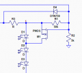
here's the circuit i'm going to order boards for. please let me know if i've got something wrong. do i have the fet's GSD labeled correctly?
since you don't show the built in diode i was unsure. most Pfet diagrams show the diode polarity toward drain. wouldn't that conduct all the time? should i reverse the source and drain?
thanks again.
upload_2017-11-11_0-21-46.png
 

Attachments

crutschow

Joined Mar 14, 2008
38,681
i think it's getting clearer on everything but gate voltage.
When the switch is up, the MOSFET source voltage is nearly equal to the gate voltage so the MOSFET is off.
When the switch is down, resistor R3 pulls the gate to ground, and the MOSFET is on.
do i have the fet's GSD labeled correctly?
since you don't show the built in diode i was unsure. most Pfet diagrams show the diode polarity toward drain. wouldn't that conduct all the time? should i reverse the source and drain?
What do you mean "the diode polarity toward the drain"? :confused:

You show the diode polarity correctly, which is the cathode to the source (the same direction as the little arrow from the center of the P-MOSFET symbol to the source).
That means the diode is reversed biased when the the MOSFET is off.
If you reversed the source and drain, then the MOSFET would be conducting all the time.
 

Thread Starter

joewales44

Joined Oct 8, 2017
218
now i understand how the gate is high or low.
what is purpose of R2? why is it necessary?
how can Vgs ever be 50 times input voltage?
i got into big trouble in the past with zeners blowing. i wasn't using TVS diodes then but am now. will this circuit be completely safe from zener failure? i have a ss14 for reverse polarity protection. when switch is up, spikes would have to go through both ss14 first. should i use 2 TVS and not go through either ss14?
and all these diodes bring up another problem, i'm running out of voltage. LED Vf is 10.5 to 11.1. with D5 and D6 it's up to 11.7. if customers have a poor switch or low battery, it runs out of voltage. i need to keep total Vf close to 11 volts. going thru D5 wouldn't hurt when LED is turned off but it's just the opposite. is there a way to make the fet work opposite the way it is now? i used a Nchannel on another project to replace D6 but prefer not to use it here if possible.
thanks to you, i'm almost there. i was getting Pchannel and Nchannel mixed up. this is my first lesson for Pchannels.
thanks again.
 

Attachments

Last edited:

crutschow

Joined Mar 14, 2008
38,681
what is purpose of R2? why is it necessary?
R2 in your schematic or mine?
how can Vgs ever be 50 times input voltage?
It can't.
That number was part of a fraction.
I stated it was 50/55 or 91% of the input voltage.
will this circuit be completely safe from zener failure?
It should be.
The zener current never exceeds 2.5mA.
going thru D5 wouldn't hurt when LED is turned off but it's just the opposite. is there a way to make the fet work opposite the way it is now? i used a Nchannel on another project to replace D6 but prefer not to use it here if possible.
What's the purpose of D6?
Why don't you want to use a FET to replace the diode as that will eliminate the diode forward voltage drop?

You could reverse the operation of the FET by adding another NPN or N-MOSFET transistor.
can i bypass middle LED like this?
No.
It messes up the bias voltages.
Why do you want to do the middle LED?
Just change the wiring order of the LEDs so the top one is the one you want to turn on and off.
 

Thread Starter

joewales44

Joined Oct 8, 2017
218
1. R2 in my schematic, the 50k. why is it necessary? by the way, 49.9k and 4.99k resistors are a lot cheaper than 50k and 5k so i will use the cheap ones.
2. not worried about zener current but damage from transients. that's what blew them in a previous design. i added tvs diodes to both inputs and both are tied directly to ground and don't go through ss14. is this enough transient protection for zeners and mosfets?
3. D6 is for reverse polarity protection. i've used a Nfet there on other boards but ss14 are cheaper. i'll see how it does with ss14 for now. i would like to see how to add a Nfet to reverse operation of Pfet. please put up a schematic.
4. i'm proud of myself, lol. i thought voltage wouldn't be high enough so i changed the wiring order.
5. i selected fets rated for 1.2A since i'll be pulling 400mA here. is it safe to pull up to their rated current? i have another board that pulls 1A that i want to use these on? the little SOT23 package scares me. Texas Instruments' rule was to always double the requirement.

i ordered 10 aluminum boards from allpcb.com for $13 and that includes shipping. i couldn't believe it. shipping is usually more than that. i'll let everyone know how good they are.
thanks
 

crutschow

Joined Mar 14, 2008
38,681
1. R2 in my schematic, the 50k. why is it necessary? by the way, 49.9k and 4.99k resistors are a lot cheaper than 50k and 5k so i will use the cheap ones.
Good question.
R2 is needed in some circuits for proper bias but it's not needed here.
The value of R4 is not critical. 4.99k is fine.
2. not worried about zener current but damage from transients. that's what blew them in a previous design. i added tvs diodes to both inputs and both are tied directly to ground and don't go through ss14. is this enough transient protection for zeners and mosfets?
Depends upon the source of the transients.
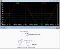
3. D6 is for reverse polarity protection. i've used a Nfet there on other boards but ss14 are cheaper. i'll see how it does with ss14 for now. i would like to see how to add a Nfet to reverse operation of Pfet. please put up a schematic.
To use a P-MOSFET for reverse polarity protection it must be in the positive lead.
If you want it to replace D6, you would use an N-MOSFET as shown below (note the source and drain connections).
As can be seen in the simulation, this prevents the load voltage, V(in,1), from going negative if the input voltage goes negative, but conducts the positive voltage will little drop.

upload_2017-11-12_9-32-4.png

5. i selected fets rated for 1.2A since i'll be pulling 400mA here. is it safe to pull up to their rated current?
For good reliability you generally don't want to pull more than about 75% of the rated current.

But it's usually the ON resistance (Vdson) that determines how large the transistor needs to be.
That will cause a voltage drop and dissipation in the MOSFET when it is ON.
You usually don't want that to generate more than about a watt of dissipation so you don't need to heatsink the MOSFET.
Thus, for example, with 1A of current, the ON resistance should be no more than 1 ohm (which will drop 1V at that current).
i ordered 10 aluminum boards
What are aluminum boards?

.
 
Last edited:

Thread Starter

joewales44

Joined Oct 8, 2017
218
1. so it's ok to completely eliminate R2? can i make R4 a 5k resistor like R3 or make them both 10k? trying to minimize parts.
2. transients will come from engine starters, pump motors, etc. with vicious load dumps. i don't know how big they are but these are what blew zeners before without TVS protection. what do you think?
3. i'm already using N mosfet for polarity protection on a different project. it's hooked up like i show in last schematic. it's working good so far. my question is - do i need both zeners or will Z1 protect Nfet gate from over voltage?
4. i'm still confused on the effect Z1 will have on driver chip. if voltage supply is 24 volts, the driver chip compensates and used less current from supply. will Z1 always hold voltage at 12v regardless of input voltage? if so, don't think i like that.
5. on resistance is 80mohm. .08ohm x .4a =.032w. is that right? here's the parts i picked.
N- http://www.mouser.com/ds/2/115/DMN6140L-709504.pdf 140mohm/2.3a
P- http://www.mouser.com/ds/2/115/DMP4065S-537770.pdf 80mohm/3.4a
seems both should be ok for 1amp. am i right?

a light came on when you explained a mosfet requires a difference in gate to source voltage, not just an input. that had never registered before.

aluminum boards are used to better dissipate heat for LEDs. you probably heard them called MCPCB or metal core boards. in higher current applications they also have DTP versions. Direct Thermal Path is where there is no dielectric layer between LED thermal pad and metal board. it has the best possible thermal transfer. only thing better is all copper board.

it feels good to tell you something, lol. didn't think it would ever happen. also know a little bit about LEDs, electronic pcb assembly, conformal coatings.
thanks
 
Top