 Facebook
 Google
 GitHub
 Linkedin
AD9833 Signal Generator
- Thread starter Vinnie90
- Start date
Scroll to continue with content
@Vinnie90So I checked the oscillation frequency with the FFT in the oscilloscope. With the LM324 the oscillations are very small and are @ 1MHz (the oscillations at the crystal). For the LM6144 the oscillations have a much wider spectrum centered around 600kHz....but also other harmonics everywhere. I tried to have a look at the layout and I couldn't find anything major that could lead to ground looping....also because the superimposed oscillations are very large in amplitude.
Did you try connecting U4D pins 13 & 14 to see if that affected the "oscillation"?
Although you believe that the LM6144 is well bypassed to ground at pins 4 & 11, have you verified the value of the bypass caps (or tried replacing them)? (caps can be defective or mismarked) I assume the caps are ceramics?
@Vinnie90I see. I still see some oscillations with the LM324 but they are way smaller in amplitude. I did a previous version of the board with the LM6144 but the PCB was wit only two layer while this new one has four.
Now, say I try to fix the cause of the oscillations...how can I test my hypothesis about the problem? Should I do several pcb versions and that would be very costly. Do you have any suggestion?
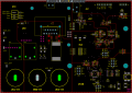
Maybe I'll attach the layout...maybe there's something very obvious that I don't see (I'm not very familiar with looking for ground loops)
The layouts you posted seem to be only a portion of the board. It is thus impossible to visually resolve grounding and other features. Can you post full layouts? (I assume, I hope, that the traces that are cut off at the edge of the images you posted are in reality not cut off.)
Right...I was just afraid that the full board would have been too much since you cannot zoom in and see the names of the nets.@Vinnie90
The layouts you posted seem to be only a portion of the board. It is thus impossible to visually resolve grounding and other features. Can you post full layouts? (I assume, I hope, that the traces that are cut off at the edge of the images you posted are in reality not cut off.)
I haven't tried that but I'll try to do it tomorrow.@Vinnie90
@Vinnie90
Did you try connecting U4D pins 13 & 14 to see if that affected the "oscillation"?
Although you believe that the LM6144 is well bypassed to ground at pins 4 & 11, have you verified the value of the bypass caps (or tried replacing them)? (caps can be defective or mismarked) I assume the caps are ceramics?
I have used 6pF active probes, with the ground wire attached a little bit further away at the output of the circuit and the waveforms are identical@Vinnie90
Also possible is the scope couples noise into the circuit.
Attachments
-
 185 KB Views: 10
 -
 225.4 KB Views: 10
 -
 228.7 KB Views: 11
 -
 197.3 KB Views: 11
@Vinnie90Right...I was just afraid that the full board would have been too much since you cannot zoom in and see the names of the nets.
I haven't tried that but I'll try to do it tomorrow.
I have used 6pF active probes, with the ground wire attached a little bit further away at the output of the circuit and the waveforms are identical
After downloading the .png images, I can zoom into them quite easily using (.e.g.) Windows Photos viewer. Thanks for posting them.
@Vinnie90
Grrr!!! After writing a full reply I accidentally clicked another Window only to find my reply had vaporized when I returned to this Window. So...here's another attempt (with many "save changes" along the way)...
To fully review your layout would require far, far more time than I can offer. However, I have reviewed the area around U4 and I offer some observations. PCB layout is both art and science. To create a good layout much knowledge and experience is needed. Online you will find many articles, books, advice, examples, etc relating to PCB layout. Because layout is a combination of both art and technical knowledge you will find online both controversy and disagreement on specific issues.
An observation:
While C12 & C13 are reasonably close to U4, the connection from the junction of C12 & C13 to GND is remote; vias that connect to the GND layer are some distance from the junction.
A suggestion:
A via (or vias) should be placed very near C12 & C13 to make connection to the GND layer. It would have been simple to place C13 on the TOP layer adjacent to U4, requiring then only one via for the ground connection to C13. The same is true of C12; only minor component placement changes would be needed to place C12 on the TOP layer (with a via to ground). Both changes would slightly reduce the length of copper from the capacitor to the relevant U4 pin, reducing the inductance of the connection. A via to the GND layer from each of C12 & C13 would provide a desired low inductance connection to ground.
Another observation:
I see on the TOP layer (I have not checked other layers) many unconnected "islands" of copper; areas of copper having no electrical connection to anything. Such areas should be forbidden; in most cases it would be appropriate to connect the islands (using vias if necessary) to the GND layer.
Some guidelines:
*The GND layer should be as contiguous (free of breaks/cuts) as possible.
*It's okay to use multiple vias when one via would technically make a connection. In fact, in the area of U4 on the BTM layer there is a large area of copper that has only a handful of vias connecting it to the GND layer; I would have expected to find a dozen (or more) vias tying that area to GND.
*If a component terminal needs to connect to ground, place a via to the GND layer as near as possible to that terminal. Exception: If multiple terminals, all needing a ground connection, are very close together (less than 0.25"), then a single via among them may be sufficient.
*PCB's having internal layers (more than TOP & BOT) are both difficult to troubleshoot and, often, almost impossible to modify when a wrong connection is found. Use as few layers as you can. If adding a few vias would eliminate the need for a layer, then use those vias.
*There is no reason why a layout should use only the narrowest traces; fit the trace width to function and current capacity. Wider traces have lower inductance but higher capacitance (to other layers). Likewise, there is no reason why a layout should place components and traces at the smallest possible separation; if there is no need for "close", don't use "close."
*As with all rules, there are times when exceptions should be made. However, make an exception only when you understand the implications of the exception and the reasons for the initial rule.
Finally, I have made no attempt to find ground loops. There is no specific reason to believe that any exist and finding them is very difficult.
Good luck!
Last edited:
Oh man, I missed the second part of the post. Super useful....I'll work on it and keep you posted@Vinnie90
After downloading the .png images, I can zoom into them quite easily using (.e.g.) Windows Photos viewer. Thanks for posting them.
@Vinnie90
Grrr!!! After writing a full reply I accidentally clicked another Window only to find my reply had vaporized when I returned to this Window. So...here's another attempt (with many "save changes" along the way)...
To fully review your layout would require far, far more time than I can offer. However, I have reviewed the area around U4 and I offer some observations. PCB layout is both art and science. To create a good layout much knowledge and experience is needed. Online you will find many articles, books, advice, examples, etc relating to PCB layout. Because layout is a combination of both art and technical knowledge you will find online both controversy and disagreement on specific issues.
An observation:
While C12 & C13 are reasonably close to U4, the connection from the junction of C12 & C13 to GND is remote; vias that connect to the GND layer are some distance from the junction.
A suggestion:
A via (or vias) should be placed very near C12 & C13 to make connection to the GND layer. It would have been simple to place C13 on the TOP layer adjacent to U4, requiring then only one via for the ground connection to C13. The same is true of C12; only minor component placement changes would be needed to place C12 on the TOP layer (with a via to ground). Both changes would slightly reduce the length of copper from the capacitor to the relevant U4 pin, reducing the inductance of the connection. A via to the GND layer from each of C12 & C13 would provide a desired low inductance connection to ground.
Another observation:
I see on the TOP layer (I have not checked other layers) many unconnected "islands" of copper; areas of copper having no electrical connection to anything. Such areas should be forbidden; in most cases it would be appropriate to connect the islands (using vias if necessary) to the GND layer.
Some guidelines:
*The GND layer should be as contiguous (free of breaks/cuts) as possible.
*It's okay to use multiple vias when one via would technically make a connection. In fact, in the area of U4 on the BTM layer there is a large area of copper that has only a handful of vias connecting it to the GND layer; I would have expected to find a dozen (or more) vias tying that area to GND.
*If a component terminal needs to connect to ground, place a via to the GND layer as near as possible to that terminal. Exception: If multiple terminals, all needing a ground connection, are very close together (less than 0.25"), then a single via among them may be sufficient.
*PCB's having internal layers (more than TOP & BOT) are both difficult to troubleshoot and, often, almost impossible to modify when a wrong connection is found. Use as few layers as you can. If adding a few vias would eliminate the need for a layer, then use those vias.
*There is no reason why a layout should use only the narrowest traces; fit the trace width to function and current capacity. Wider traces have lower inductance but higher capacitance (to other layers). Likewise, there is no reason why a layout should place components and traces at the smallest possible separation; if there is no need for "close", don't use "close."
*As with all rules, there are times when exceptions should be made. However, make an exception only when you understand the implications of the exception and the reasons for the initial rule.
Finally, I have made no attempt to find ground loops. There is no specific reason to believe that any exist and finding them is very difficult.
Good luck!
")
Thanks a lot for the advice and the help
Vince
If you look at phase gain curves this opamp is a recipe for Cload oscillation and/or
feedback stray C at inv node input because of phase margin problems. LM324
is unity G comped, has no such issues.

When you place a scope probe at inv input you are adding a 3'rd pole to this control
loop. Especially if your probe set to X1. A huge bad idea unless you have a FET probe
with a couple of pF or less input C.
It does show a Cload of 100 pF but very low phase margin loaded like that, add a few
pF or high fdbk R to inv node and you have a RF oscillator and can toss the DDS chips
So key is layout minimize inv node stray C, output load C, lower fdbk R absolute values
where ever possible.
Also caps critical. Not every ceramic .01 and .1 have same ESR, some can be crappy
due to package lead L. That's a killer, so closely examine datasheet. Set up a jig on a
bare PCB with a 50 ohm series R to cap to ground, drive that with a signal generator,
and look at how good/bad the ESR is. You will be surprised. One manufacturer to another.
Additionally if you start dropping G setting R values to move the parasitic pole you are
creating at inv input that takes more current / drive out of the OpAmp. So you may need
some bulk C on the OpAmps as well
Not all bulk C technologies perform the same as you can see here -

https://www.eetimes.com/author.asp?section_id=36&doc_id=1330842
https://www.analog.com/media/en/technical-documentation/application-notes/an47fa.pdf
Regards, Dana.
feedback stray C at inv node input because of phase margin problems. LM324
is unity G comped, has no such issues.
When you place a scope probe at inv input you are adding a 3'rd pole to this control
loop. Especially if your probe set to X1. A huge bad idea unless you have a FET probe
with a couple of pF or less input C.
It does show a Cload of 100 pF but very low phase margin loaded like that, add a few
pF or high fdbk R to inv node and you have a RF oscillator and can toss the DDS chips
So key is layout minimize inv node stray C, output load C, lower fdbk R absolute values
where ever possible.
Also caps critical. Not every ceramic .01 and .1 have same ESR, some can be crappy
due to package lead L. That's a killer, so closely examine datasheet. Set up a jig on a
bare PCB with a 50 ohm series R to cap to ground, drive that with a signal generator,
and look at how good/bad the ESR is. You will be surprised. One manufacturer to another.
Additionally if you start dropping G setting R values to move the parasitic pole you are
creating at inv input that takes more current / drive out of the OpAmp. So you may need
some bulk C on the OpAmps as well
Not all bulk C technologies perform the same as you can see here -
https://www.eetimes.com/author.asp?section_id=36&doc_id=1330842
https://www.analog.com/media/en/technical-documentation/application-notes/an47fa.pdf
Regards, Dana.
Last edited:
@Vinnie90So I checked the oscillation frequency with the FFT in the oscilloscope. With the LM324 the oscillations are very small and are @ 1MHz (the oscillations at the crystal). For the LM6144 the oscillations have a much wider spectrum centered around 600kHz....but also other harmonics everywhere. I tried to have a look at the layout and I couldn't find anything major that could lead to ground looping....also because the superimposed oscillations are very large in amplitude.
Other observations:
W2 of U2A has a range of +3V to -3V. This seems excessive to me considering that the output of U4C:8 is only offset by about +0.35V. Perhaps add a resistor divider between U2A:15 and U4D:12, with a cap bypass to ground at U4D:12? Whether excessive or not (according to your goal), currently most of the noise on your +/-3V supplies could potentially appear at U4D:12, creating unwanted feedback via the +/-3V supplies. A bypass cap to ground at U4D:12 is definitely needed.
When using a rail-to-rail op-amp, you need to consider that when the output is at max or min, then anything (noise, coupling to another device) on the power supply rail(s) or on ground is essentially tied directly to the op-amp output. That is, care is needed if your design allows any rail-to-rail op-amp to reach min or max output...even in an unusual condition (e.g. power up); proper bypass and regulation of power supplies can become very important. Without care (and too often even with care) it is possible for a power supply or ground connection to inadvertently/undesirably couple two points that must remain independent of each other.
Properly grounding components on a PCB layout can be quite challenging for complex circuits. As a rule-of-thumb, using a ground plane is a good starting point. However, rules-of-thumb for PCB layout are like other recommendations; they help you when you don't know what you are doing or you don't have initiative/time/money/knowledge to figure out why the rule exists. If you do know what you are doing, then rules lose their value. If you really understand what you are doing, you may well act in a manner that is superior to following the rule.
Hi folks,
back with some updates on the project. I have been working trying to figure out what the problem was. I have implemented some of your suggestions where possible in the new PCB:
- better grounding in the layout between the top and bottom layer with the addition of arrays of GND vias.
- Analog bypass capacitor on the same layer of the component and as close as possible.
- Checked the value for the bypass by looking at the ESR of the datasheet. The main source of noise in my system is given by a XCO at 1MHz. The value of capacitors seem to be working both theoretically and experimentally (Added an additional 10uF to U4 which seems to be the more vulnerable in the system).
- Following @danadak's suggestions I have improved the probing by using an active probe (8pF with grounding with a very short lead, see picture).
- Following @TeeKay6 suggestions I have added a small bypass at pin5 of U4 where the problem seems to be arising
I'm attaching a .pdf with the full schematic and layout for clarity.
NB1. In the PCB I have connected pin3 of U4 directly to ground and do not have U3 (AD5260 desoldered).
NB2. In the schematics the decoupling capacitors are usually at the bottom left of the page.
OUTCOME:
I have tried to generate a 1kHz sinewave with a controllable amplitude.
- Overall way better bypassing of the harmonics coming from the XCO to the analog part of the system.
- However, my sinewave is still randomly oscillating after the first buffering stage.
DEBUGGING:
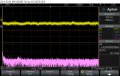
Following the signal from the AD9833 to the final output I have taken some snapshots of the the signal in time and frequency domain (see attached pictures). The sinewave generated from the AD9833 is nice and smooth at the output of the buffer stage (pic pin10_1khz) with only a little bit of the 1MHz clock entering (pic pin10_1mhz) with around 60dB attenuation with respect to the sine wave.
Immediately after the buffering stage there is a spurious ~570kHz+2nd, 3rd ect. harmonics (although not very distorted) entering the opamp (picture pin6_1, pin6_2). Pin5 of U4 does not show any show any signs of those frequencies (pic pin5) nor supplies (pic vdd and vss). n addition at pin 6 there is no sign of the original 1kHz sinewave.
Following the signal through the voltage divider to pin12 of U4 the original 1kHz sinewave reappears with high amplitude noise superimposed(pic pin12_1). The FFT shows that this noise is at around 1MHz and with two minor peaks 1MHz +/- 32kHz (pic pin12_2, like some sort of frequency modulation). Output at pin14 is exactly the same but amplified of a factor 10.
I have no other digital component working (e.g. no SPI or USB communication).
Any thoughts?
Thanks a ton for the help
Schematics in the following post
back with some updates on the project. I have been working trying to figure out what the problem was. I have implemented some of your suggestions where possible in the new PCB:
- better grounding in the layout between the top and bottom layer with the addition of arrays of GND vias.
- Analog bypass capacitor on the same layer of the component and as close as possible.
- Checked the value for the bypass by looking at the ESR of the datasheet. The main source of noise in my system is given by a XCO at 1MHz. The value of capacitors seem to be working both theoretically and experimentally (Added an additional 10uF to U4 which seems to be the more vulnerable in the system).
- Following @danadak's suggestions I have improved the probing by using an active probe (8pF with grounding with a very short lead, see picture).
- Following @TeeKay6 suggestions I have added a small bypass at pin5 of U4 where the problem seems to be arising
I'm attaching a .pdf with the full schematic and layout for clarity.
NB1. In the PCB I have connected pin3 of U4 directly to ground and do not have U3 (AD5260 desoldered).
NB2. In the schematics the decoupling capacitors are usually at the bottom left of the page.
OUTCOME:
I have tried to generate a 1kHz sinewave with a controllable amplitude.
- Overall way better bypassing of the harmonics coming from the XCO to the analog part of the system.
- However, my sinewave is still randomly oscillating after the first buffering stage.
DEBUGGING:
Following the signal from the AD9833 to the final output I have taken some snapshots of the the signal in time and frequency domain (see attached pictures). The sinewave generated from the AD9833 is nice and smooth at the output of the buffer stage (pic pin10_1khz) with only a little bit of the 1MHz clock entering (pic pin10_1mhz) with around 60dB attenuation with respect to the sine wave.
Immediately after the buffering stage there is a spurious ~570kHz+2nd, 3rd ect. harmonics (although not very distorted) entering the opamp (picture pin6_1, pin6_2). Pin5 of U4 does not show any show any signs of those frequencies (pic pin5) nor supplies (pic vdd and vss). n addition at pin 6 there is no sign of the original 1kHz sinewave.
Following the signal through the voltage divider to pin12 of U4 the original 1kHz sinewave reappears with high amplitude noise superimposed(pic pin12_1). The FFT shows that this noise is at around 1MHz and with two minor peaks 1MHz +/- 32kHz (pic pin12_2, like some sort of frequency modulation). Output at pin14 is exactly the same but amplified of a factor 10.
I have no other digital component working (e.g. no SPI or USB communication).
Any thoughts?
Thanks a ton for the help
Schematics in the following post
Attachments
-
 183.6 KB Views: 11
 -
 35.1 KB Views: 10
 -
 36.4 KB Views: 8
 -
 71.7 KB Views: 8
 -
 36.6 KB Views: 9
 -
 34.9 KB Views: 9
 -
 60.5 KB Views: 8
 -
 63.5 KB Views: 7
 -
 34.6 KB Views: 8
 -
 34.9 KB Views: 7
Last edited:
Schematic and layout. The schematic related to the section I was talking about is the Signal generator page (pg.4)
Attachments
-
1.2 MB Views: 18
-
37.5 KB Views: 5
Last edited:
@Vinnie90Schematic and layout. The schematic related to the section I was talking about is the Signal generator page (pg.4)
In a previous post I said "W2 of U2A has a range...between U2A:15 and U4D:12, with a cap bypass to ground at U4D:12? ... could potentially appear at U4D:12... A bypass cap to ground at U4D:12 is definitely needed." Wow, I really scrambled that paragraph! The pin needing a bypass is U4B:5. You corrected my error and added C15 from U4B:5/U2A:15. Good!
More later...
In some snapshots I increased the time base to show more clearly the signal in the time domain, but thanks for the suggestionYour FFT, you need to set timebase for more cycles to get better
resolution and measurements.
I'm afraid I don't get this point? Where's the brick?Power from a brick ? Try with a grounded bench top supply. Looks
like you have a lot of 60 Hz in one of the screenshots.
Anyway I tried both to power the system from the onboard LM27762 and bench top power supplies (which are the one in the pictures). No difference in the outputs. Not at all @TeeKay6, you were right!!! In the previous version the DC_OFF was connected to pin12. I shuffled a bit the connections in this new version to give the signal the shortest path possible between pins.In a previous post I said "W2 of U2A has a range...between U2A:15 and U4D:12, with a cap bypass to ground at U4D:12? ... could potentially appear at U4D:12... A bypass cap to ground at U4D:12 is definitely needed." Wow, I really scrambled that paragraph! The pin needing a bypass is U4B:5. You corrected my error and added C15 from U4B:5/U2A:15. Good!
@Vinnie90In some snapshots I increased the time base to show more clearly the signal in the time domain, but thanks for the suggestion
I'm afraid I don't get this point? Where's the brick?
Not at all @TeeKay6, you were right!!! In the previous version the DC_OFF was connected to pin12. I shuffled a bit the connections in this new version to give the signal the shortest path possible between pins.
My suggestion is that we must cut the connection from U4B:7 to U2A:2 so that we can see what U4B does with no load other than RA1. This will eliminate any effect that U2A is having on U4B. There is something going on with U4B that we have not yet touched. If you have already tried this (e.g. cutting the trace as near to pin7 as is easily feasible), tell me what you saw. Otherwise, please make the cut (hopefully where you can patch it later) and report what effect that had.
As an aside, relating to PCB layout, I call your attention to the layout around RA1. In the schematic, note the connections of the RA1 pins. Pin2 connects to U4C:8, a low impedance output. Pin1 connects to U4B:7, a low impedance output. Pins 3 & 4 connect to U4B:6--a high impedance input. So, what would likely be the preferred layout compromise?: (a) make the RA1:2 trace as short as possible. (b) make the RA1:1 trace as short as possible. (c) make the RA1:3,4 trace as short as possible. If you guess that (a) or (b) are better than (c), then you lose...and that is what you chose to do in the PCB layout, to attach a large antenna trace to RA1:3,4. (Also to consider: You do not want RA1:1 and RA1:3.4 traces to have a long parallel run and thus high capacitance between them, nor--for the same reason--do you want parallel traces to RA1:2 and RA1:3,4.) This is not a grievous error but it does show that you were not paying enough attention when you were connecting RA1. For low frequencies, or with a low bandwidth opamp, this would likely have little/no effect, but with a high-speed opamp it could have significant effect. Now, please don't rush to amend the layout unless we can actually show a bad effect in this case.
I'll try to desolder U2 first and connect pin5 of U4 to ground (simple inverting amplifier with unity gain) and I'll tie pin8 with pin12 directly changing R2 from 100k to 10k (non inverting amplifier with unity gain).@Vinnie90
My suggestion is that we must cut the connection from U4B:7 to U2A:2 so that we can see what U4B does with no load other than RA1. This will eliminate any effect that U2A is having on U4B. There is something going on with U4B that we have not yet touched. If you have already tried this (e.g. cutting the trace as near to pin7 as is easily feasible), tell me what you saw. Otherwise, please make the cut (hopefully where you can patch it later) and report what effect that had.
Never thought about it. It's actually super useful and I'll try to implement this in all my future layouts. Unfortunately PCB routing has a lot of untold rules that no one tells you at school.As an aside, relating to PCB layout, I call your attention to the layout around RA1. In the schematic, note the connections of the RA1 pins. Pin2 connects to U4C:8, a low impedance output. Pin1 connects to U4B:7, a low impedance output. Pins 3 & 4 connect to U4B:6--a high impedance input. So, what would likely be the preferred layout compromise?: (a) make the RA1:2 trace as short as possible. (b) make the RA1:1 trace as short as possible. (c) make the RA1:3,4 trace as short as possible. If you guess that (a) or (b) are better than (c), then you lose...and that is what you chose to do in the PCB layout, to attach a large antenna trace to RA1:3,4. (Also to consider: You do not want RA1:1 and RA1:3.4 traces to have a long parallel run and thus high capacitance between them, nor--for the same reason--do you want parallel traces to RA1:2 and RA1:3,4.) This is not a grievous error but it does show that you were not paying enough attention when you were connecting RA1. For low frequencies, or with a low bandwidth opamp, this would likely have little/no effect, but with a high-speed opamp it could have significant effect. Now, please don't rush to amend the layout unless we can actually show a bad effect in this case.
Keep you posted!
Sooo I'm very happy because I think that following the tips of @TeeKay6 I found the issue!!!!
I have disconnected U2 from the PCB. soldered pin 2 and 3 of U2 together and tied pin 5 of U4 to ground. I also lowered the gain of U4D by changing R2 from 100k to 10k. No luck....still oscillations around 500kHz.
Then to test @TeeKay6's hypothesis instead of soldering together pin 2 and 3 I soldered together pin 3 and 4 of U2 (which means pin12 of U4 to ground), to exclude the last section of the quad opamp. I soldered also a 10k resistor between pin7 and ground and.....voila no more oscillations.
To my understanding this confirms Teekay's hypothesis that the two long traces between pin7 and pin 12 of U4 are working as antenna picking up random noise.
@Vinnie90Sooo I'm very happy because I think that following the tips of @TeeKay6 I found the issue!!!!
I have disconnected U2 from the PCB. soldered pin 2 and 3 of U2 together and tied pin 5 of U4 to ground. I also lowered the gain of U4D by changing R2 from 100k to 10k. No luck....still oscillations around 500kHz.
Then to test @TeeKay6's hypothesis instead of soldering together pin 2 and 3 I soldered together pin 3 and 4 of U2 (which means pin12 of U4 to ground), to exclude the last section of the quad opamp. I soldered also a 10k resistor between pin7 and ground and.....voila no more oscillations.
To my understanding this confirms Teekay's hypothesis that the two long traces between pin7 and pin 12 of U4 are working as antenna picking up random noise.
Whoa! Your conclusions are jumping beyond your data. Let's review what you've done, step by step.
First, you "disconnected U2 from the PCB. soldered pin 2 and 3 of U2 together and tied pin 5 of U4 to ground. I also lowered the gain of U4D by changing R2 from 100k to 10k." You found a high freq oscillation still present (at U4B?). You have thus shown: It is not necessary for U2A to be in the circuit for U4B to show the oscillation. That is an unequivocal conclusion. However, you chose to keep U4D actively amplifying the signal at U4B:7, rather than letting U4D:12 be tied to ground via pins 3 & 4 of U2A. My only suggestion to you was to disconnect U2A:2 from U4B:7.
Next, "instead of soldering together pin 2 and 3 I soldered together pin 3 and 4 of U2 (which means pin12 of U4 to ground),..." and--WHY?--you "soldered also a 10k resistor between pin7 and ground." (Perhaps you intended to simulate the load of U2A on U4B:7? Is the pot of U2A a 10K pot?) You now saw no oscillation. Hmm, do you remember reading in another post my suggestion that when troubleshooting you try to change only one thing at a time? Do you remember reading in another post my suggestion that it is unwise to jump to conclusions without supporting data? So, one possible conclusion at this point is that by changing the circuitry around U4D you managed to kill the Evil Purple Worm that was causing the oscillation. An equally valid conclusion is that by adding the 10K resistor to ground from U4B:7, you upset the Oscillation Monster and he decided to withdraw, taking his oscillation with him. Or perhaps the Oscillation Monster depended on the Evil Purple Worm and now that the Worm was dead, the Oscillation Monster also died. Or perhaps the parallel traces to U4B:7 and U4D:12 are somehow involved...or not. Or perhaps it was the trace from U4B:7 transmitting to the trace at RA1:2 that caused the problem? Or perhaps... The point is that at this stage you have proven only one thing: the oscillation is gone after you made all your changes. That is useful information, but does not lead to a definite conclusion. We do know that something you did was indeed effective in killing the oscillation. What we don't know is of those things you did, which led to the desirable outcome. Now think along this line for a moment: the trace from U4B:7 is a low impedance output from the opamp. The trace from U4D:12 is a high impedance input pin of an opamp. So, indeed, there is a possibility of U4B:7 transmitting and U4D:12 receiving. However...that is what is intended to happen anyway, although via W1 of U2A. So why would that transmit-receive cause a problem? Also, for an oscillation to be sustained in U4B there must be some path from a later point back to an earlier point in the signal path. Where is that feedback path? Now...I am being deliberately conclusive (for teaching purposes) when I have no real justification for being so certain. Nevertheless, my reason tells me that it is at least unlikely that the transmit-receive we have hypothesized is causing a problem; however, I can indeed be wrong! We are far from having proved that it is causing a (or the) problem.
So one reasonable next step would be to first undo your multiple changes to a state where the oscillation is again present (I believe that means: U2A absent, U2A:2 and U2A:3 tied together, R2=100K.) I believe that you have indeed shown that U2A need not be connected to U4B:7 for oscillation to be present, so there is no need to reinstall U2A yet. With the circuit again oscillating, let's now make changes--one at a time!--and see what is the effect of each. I suggest that one easy change would be to replace the 10K resistor from U4B:7 to ground (in the same location you had used previously). Did that abolish the oscillation? If yes, that is a nice clue. If no, then remove the 10K resistor. Next, I suggest disconnecting U4B:2 from U4B:3; instead connect U4B:3 to U4B:4, leaving U4B:2 unconnected. Is the oscillation still present? If yes, that means the circuit can oscillate with no coupling (other than inductive--still a possibility OR via a ground/PS coupling) into U4D:12; however, we don't yet know whether U4D is involved in some other manner (U4B and U4D are, after all, in the same IC package, sharing power and ground connections as well as close proximity of pins). If the oscillation is now absent, then we know that the U4D stage is somehow implicated and that coupling from U4D:12 to U4B:7 (via U2A) is necessary for the oscillation to persist.
Try to repeat your testing up to the point I have just described and let me know the results. We will then decide what are good things to try next.
Good luck! By the way, ask any electronics engineer and they will tell you that debugging hardware is their least favorite engineering task.
Last edited:
@Vinnie90@Vinnie90
Whoa! Your conclusions are jumping beyond your data. Let's review what you've done, step by step.
First, you "disconnected U2 from the PCB. soldered pin 2 and 3 of U2 together and tied pin 5 of U4 to ground. I also lowered the gain of U4D by changing R2 from 100k to 10k." You found a high freq oscillation still present (at U4B?). You have thus shown: It is not necessary for U2A to be in the circuit for U4B to show the oscillation. That is an unequivocal conclusion. However, you chose to keep U4D actively amplifying the signal at U4B:7, rather than letting U4D:12 be tied to ground via pins 3 & 4 of U2A. My only suggestion to you was to disconnect U2A:2 from U4B:7.
Next, "instead of soldering together pin 2 and 3 I soldered together pin 3 and 4 of U2 (which means pin12 of U4 to ground),..." and--WHY?--you "soldered also a 10k resistor between pin7 and ground." (Perhaps you intended to simulate the load of U2A on U4B:7? Is the pot of U2A a 10K pot?) You now saw no oscillation. Hmm, do you remember reading in another post my suggestion that when troubleshooting you try to change only one thing at a time? Do you remember reading in another post my suggestion that it is unwise to jump to conclusions without supporting data? So, one possible conclusion at this point is that by changing the circuitry around U4D you managed to kill the Evil Purple Worm that was causing the oscillation. An equally valid conclusion is that by adding the 10K resistor to ground from U4B:7, you upset the Oscillation Monster and he decided to withdraw, taking his oscillation with him. Or perhaps the Oscillation Monster depended on the Evil Purple Worm and now that the Worm was dead, the Oscillation Monster also died. Or perhaps the parallel traces to U4B:7 and U4D:12 are somehow involved...or not. Or perhaps it was the trace from U4B:7 transmitting to the trace at RA1:2 that caused the problem? Or perhaps... The point is that at this stage you have proven only one thing: the oscillation is gone after you made all your changes. That is useful information, but does not lead to a definite conclusion. We do know that something you did was indeed effective in killing the oscillation. What we don't know is of those things you did, which led to the desirable outcome. Now think along this line for a moment: the trace from U4B:7 is a low impedance output from the opamp. The trace from U4D:12 is a high impedance input pin of an opamp. So, indeed, there is a possibility of U4B:7 transmitting and U4D:12 receiving. However...that is what is intended to happen anyway, although via W1 of U2A. So why would that transmit-receive cause a problem? Also, for an oscillation to be sustained in U4B there must be some path from a later point back to an earlier point in the signal path. Where is that feedback path? Now...I am being deliberately conclusive (for teaching purposes) when I have no real justification for being so certain. Nevertheless, my reason tells me that it is at least unlikely that the transmit-receive we have hypothesized is causing a problem; however, I can indeed be wrong! We are far from having proved that it is causing a (or the) problem.
So one reasonable next step would be to first undo your multiple changes to a state where the oscillation is again present (I believe that means: U2A absent, U2A:2 and U2A:3 tied together, R2=100K.) I believe that you have indeed shown that U2A need not be connected to U4B:7 for oscillation to be present, so there is no need to reinstall U2A yet. With the circuit again oscillating, let's now make changes--one at a time!--and see what is the effect of each. I suggest that one easy change would be to replace the 10K resistor from U4B:7 to ground (in the same location you had used previously). Did that abolish the oscillation? If yes, that is a nice clue. If no, then remove the 10K resistor. Next, I suggest disconnecting U4B:2 from U4B:3; instead connect U4B:3 to U4B:4, leaving U4B:2 unconnected. Is the oscillation still present? If yes, that means the circuit can oscillate with no coupling (other than inductive--still a possibility OR via a ground/PS coupling) into U4D:12; however, we don't yet know whether U4D is involved in some other manner (U4B and U4D are, after all, in the same IC package, sharing power and ground connections as well as close proximity of pins). If the oscillation is now absent, then we know that the U4D stage is somehow implicated and that coupling from U4D:12 to U4B:7 (via U2A) is necessary for the oscillation to persist.
Try to repeat your testing up to the point I have just described and let me know the results. We will then decide what are good things to try next.
Good luck! By the way, ask any electronics engineer and they will tell you that debugging hardware is their least favorite engineering task.
Another approach: Condensing all the blah, blah, blah of my previous post: As I reread your post, you showed that with U4D:12 connected to U4B:7 via U2A:2 & U2A:3 tied together and R2=10K there is oscillation. You then showed that, starting from that first configuration, if you add a 10K resistor from U4B:7 to ground (where?) and also move the connection of U2A pins 2 & 3 to, instead, pins 3 & 4, there is no oscillation. I suggest that the best next step, while the circuit is still not oscillating, is to remove the 10K resistor from U4B:7. What is the effect of that removal, oscillation or no oscillation? If oscillation returned, then that 10K is a good clue, and the next step would depend on that. On the other hand, if oscillation did not return, leave the 10K removed (as being irrelevant). If I remember correctly, we had some time ago tried a test in which you set W1 at B1 (via U2A chip) and found, at that time, that the oscillation persisted. That configuration would be very close to the present configuration except that U2A would not present a direct short between its pins 3 &4; instead there would be the W1 wiper resistance between those pins, small but definitely not zero ohms, plus any coupling internal to the AD5262. Thus we are now trying to understand how U4D circuitry supports oscillation. Following your hunch of capacitive coupling from U4B:7 to U4D:12 due to parallel traces, I suggest that a reasonable next step would be to replace the short between U2A:3 and U2A:4 with a resistor (very short leads, or SMD) to simulate wiper resistance. An exact value is not given in the AD5262 datasheet, but my guess is that 100Ω would be a reasonable "typical" value for ±3.3V operation (however, testing with a 330Ω resistor would not be unreasonable as worst case). With that resistor in place of the direct short, does the oscillation return? If the oscillation returns, that is one confirmation of your hunch, but we need more. The next steps would be trying to determine how the U4D stage is a part of the positive feedback path that supports oscillation. Such determination is made difficult by U4B and U4D being parts of the same IC. It is relevant that your changing R2 from 100K to 10K did not eliminate the oscillation.
Last edited:
Thanks @TeeKay6 for the explanation. Yes probably I have been very optimistic in claiming I found the issue as all your point of concerns are definitely true.
Following your advice I have desoldered the 10k from pin7 to ground and measured the voltage output at pin7 of U4. Crazy oscillations...
As next step I was thinking of cutting completely the trace going out from pin7 of U4 as close as to the pin as possible and do the same with trace from pin12 and do an external patching with a short wire. To check the full system without U2 but with all connections
My rational here was to see whether keeping the system identical with the removal of U2 would keep oscillating or would stop. Instead of adding something little by little (probably the most intelligent approach) I decided to remove something from the system piece by pieceFirst, you "disconnected U2 from the PCB. soldered pin 2 and 3 of U2 together and tied pin 5 of U4 to ground. I also lowered the gain of U4D by changing R2 from 100k to 10k." You found a high freq oscillation still present (at U4B?). You have thus shown: It is not necessary for U2A to be in the circuit for U4B to show the oscillation. That is an unequivocal conclusion. However, you chose to keep U4D actively amplifying the signal at U4B:7, rather than letting U4D:12 be tied to ground via pins 3 & 4 of U2A. My only suggestion to you was to disconnect U2A:2 from U4B:7
At this point I wanted to prove that the problem was indeed the long connection between pin7 of U4 and pin2 of U2. By adding a 10k (through hole resistor soldered directly at the IC pin and a ground via nearby) I wanted to see whether providing a ground path to the signal would stop oscillations. However, I have not provided the counter experiment, that is U4B disconnected from U4D with no loadNext, "instead of soldering together pin 2 and 3 I soldered together pin 3 and 4 of U2 (which means pin12 of U4 to ground),..." and--WHY?--you "soldered also a 10k resistor between pin7 and ground." (Perhaps you intended to simulate the load of U2A on U4B:7? Is the pot of U2A a 10K pot?) You now saw no oscillation.
Following your advice I have desoldered the 10k from pin7 to ground and measured the voltage output at pin7 of U4. Crazy oscillations...
As next step I was thinking of cutting completely the trace going out from pin7 of U4 as close as to the pin as possible and do the same with trace from pin12 and do an external patching with a short wire. To check the full system without U2 but with all connections
Last edited:
@Vinnie90Thanks @TeeKay6 for the explanation. Yes probably I have been very optimistic in claiming I found the issue as all your point of concerns are definitely true.
My rational here was to see whether keeping the system identical with the removal of U2 would keep oscillating or would stop. Instead of adding something little by little (probably the most intelligent approach) I decided to remove something from the system piece by piece
At this point I wanted to prove that the problem was indeed the long connection between pin7 of U4 and pin2 of U2. By adding a 10k (through hole resistor soldered directly at the IC pin and a ground via nearby) I wanted to see whether providing a ground path to the signal would stop oscillations. However, I have not provided the counter experiment, that is U4B disconnected from U4D with no load
Following your advice I have desoldered the 10k from pin7 to ground and measured the voltage output at pin7 of U4. Crazy oscillations...
As next step I was thinking of cutting completely the trace going out from pin7 of U4 as close as to the pin as possible and do the same with trace from pin12 and do an external patching with a short wire. To check the full system without U2 but with all connections
Do not become discouraged if my remarks seem critical; you are doing quite well. My intent is to educate and to elucidate my thinking...that is certainly not always more correct than yours. Your initiative to try new experiments is definitely a plus.
You say "Following your advice I have desoldered the 10k from pin7 to ground and measured the voltage output at pin7 of U4. Crazy oscillations..." Since you did not clarify whether the oscillations were present or not prior to removing the 10K, it is impossible for me to interpret what effect the 10K had. Can you now clarify whether the circuit oscillation changed solely due adding/removing the 10K?
Your concern about the length & placement of the trace from U4B:7 to U2A:2 is certainly valid. Adding the 10K resistor added length to what already existed.
Our goals include:
(1) Finding something, anything, that clearly affects the oscillation. You have thus far successfully shown that removing U2A does not prevent oscillation, that connecting U2B:7 to U2D:12 allows oscillation, that grounding U4D:12 does stop oscillation (is that true?), that grounding U4B:5 (alone; no other changes) does not prevent oscillation. That is considerably more than we knew a few days ago. Once I understand your statement about removing the 10K, we may add another bit of knowledge to the list...perhaps a very important bit.
(2) Finding a way to prevent the oscillation while allowing desired circuit operation. We're still looking for this.
I anxiously await you answer regarding the 10K removal.
Last edited:


