Active load - strange fall time

Thread Starter

Andrius B.

Joined May 6, 2017
20
Hello,
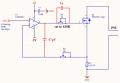
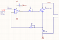
I am designing this active load circuit with opamp and MOSFET. Opamp is controlling MOSFET conductivity by what is applied to its input.


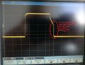
I attach oscilogram. It it taken at MOSFET gate. The rise time is good, but fall time is strange.. It fells like there is some capacitance discharging. By varying feedback resistor R11 i can slide the portion of the falling slope a bit, but i can't make it look nice as rise time.
Can you help me? How to make falltime look clean? I wish rise and falltime to be <200ns
 

Attachments

AlbertHall

Joined Jun 4, 2014
12,347
What value was R2 set to when you took that waveform?
The input capacitance of the MOSFET is around 1nF so R2 forms a low pass filter which will slow the edges. The opamp output only goes a little way below the gate threshold of the MOSFET so adding the capacitor across R2 speeds up the falling edge of the waveform (rising edge too!) so, to some extent, negating that low pass filter.
 

Thread Starter

Andrius B.

Joined May 6, 2017
20
This makes sense :) The value of R2 was about 700 ohms. R11 is set to 1K. But why R11 controls only falling edge timing?
 

AnalogKid

Joined Aug 1, 2013
11,055
I wish rise and falltime to be <200ns
Similar to a bipolar transistor in concept, the transfer function of a MOSFET is nonlinear. Also, the circuit has an asymmetrical output impedance driving R16. On the positive edge, Q1 is turned on hard as its gate is overdriven past what is needed for full enhancement, and its 17 mohm resistance is significantly lower than R16. On the negative edge Q1 is turning off, its Rds is increasing, but the gate is not overdriven in the other direction ( to -3 V) to suck out the gate charge as fast as it was pumped in.

ak
 

Thread Starter

Andrius B.

Joined May 6, 2017
20
Similar to a bipolar transistor in concept, the transfer function of a MOSFET is nonlinear. Also, the circuit has an asymmetrical output impedance driving R16. On the positive edge, Q1 is turned on hard as its gate is overdriven past what is needed for full enhancement, and its 17 mohm resistance is significantly lower than R16. On the negative edge Q1 is turning off, its Rds is increasing, but the gate is not overdriven in the other direction ( to -3 V) to suck out the gate charge as fast as it was pumped in.

ak
Thanks for reply. What could you advise to correct the falling edge? Maybe power opamp from negative supply instead of ground?
 

AnalogKid

Joined Aug 1, 2013
11,055
What I forgot to say before that explanation is that the waveshapes at the gate and at the drain are very different. What is the waveform at the drain?

ak
 

Thread Starter

Andrius B.

Joined May 6, 2017
20
What I forgot to say before that explanation is that the waveshapes at the gate and at the drain are very different. What is the waveform at the drain?

ak
Drain is connected to the lab power supply, so the waveform will be dc voltage plus some transients at the current pulse edges.Maybe I should look at the source which is connected to current sense reaistor?
 

AnalogKid

Joined Aug 1, 2013
11,055
The transient response characteristics of the power supply under test directly affect the waveform presented to the Q1 gate.

ak
 

Thread Starter

Andrius B.

Joined May 6, 2017
20
The transient response characteristics of the power supply under test directly affect the waveform presented to the Q1 gate.

ak
So that means if I connect a crappy power supply with bad transient response to my electronic load, a current waveform would look bad too? Test equipement should be independent of devices under test :)
 

AnalogKid

Joined Aug 1, 2013
11,055
The test equipment is in series with the device under test, not powering it through a zero-ohm output impedance power supply. The whole idea of transient testing a power supply is to see how it behaves during the transient condition, like turning a load on or off in 200 ns. The DUT supplies the current through R16, so it and its frequency response characteristics are *inside* the opamp feedback loop. That has consequences. If you put a good and a bad (whatever those terms mean in this context) supply through the same tests and record the gate waveforms, they will be different.

ak
 

Thread Starter

Andrius B.

Joined May 6, 2017
20
The test equipment is in series with the device under test, not powering it through a zero-ohm output impedance power supply. The whole idea of transient testing a power supply is to see how it behaves during the transient condition, like turning a load on or off in 200 ns. The DUT supplies the current through R16, so it and its frequency response characteristics are *inside* the opamp feedback loop. That has consequences. If you put a good and a bad (whatever those terms mean in this context) supply through the same tests and record the gate waveforms, they will be different.

ak
How would you improve circuit to make falltime faster and more like risetime? Or should I don`t care about gate waveform and try to get nice waveform on source? Tomorrow I will try a few tests:
-conecting different psu under test, maybe a 12v 7ah lead acid battery
- try a 2nF cap across R2
-try powering opamp with negative rail
-increasing R16.
Maybe you can share some more ideas?
 

AnalogKid

Joined Aug 1, 2013
11,055
If the goal is to have a fast reduction in load current, then the load current waveform (across R16) should be the focus. If you don't know what that is, how do you know there is a problem to address?

ak
 

Thread Starter

Andrius B.

Joined May 6, 2017
20
I have modified schematic a bit. Please see picture Opamp_FET. Now opamp is more stable. But there a things that i cannot find explanation, maybe you could help :

1) The actual Voltage on sense resistor is about 25 smaller that set voltage.. Where is it wasted? Is it on MOSFET Rds? (see picture "smaller amplitude")

2) There is a delay between signal generator voltage rising edge (set current) and actual current wavevorm rising edge.The higher the current the smaller the delay. With very small current the delay gets bigger.. Why? (se pictures Delay1, Delay2)

3) Please see picture "MOSFET turns off". Mosfet current falls to zero at point when signal generator output falls down. It's good. But gate voltage at this point is still higher than required to keep mosfet turned on. Why does it turn off?
 

Attachments

ronv

Joined Nov 12, 2008
3,770
I have modified schematic a bit. Please see picture Opamp_FET. Now opamp is more stable. But there a things that i cannot find explanation, maybe you could help :

1) The actual Voltage on sense resistor is about 25 smaller that set voltage.. Where is it wasted? Is it on MOSFET Rds? (see picture "smaller amplitude")

2) There is a delay between signal generator voltage rising edge (set current) and actual current wavevorm rising edge.The higher the current the smaller the delay. With very small current the delay gets bigger.. Why? (se pictures Delay1, Delay2)

3) Please see picture "MOSFET turns off". Mosfet current falls to zero at point when signal generator output falls down. It's good. But gate voltage at this point is still higher than required to keep mosfet turned on. Why does it turn off?
1-Only a guess.. I suspect it is measurement error and they are the same.
2- This is due to the 47pf cap slowing down the edge.
3- The whole circuit runs at the FET threshold voltage. So the instant the FET turns off the op amp is happy.
I'm pretty sure this isn't what you want to hear. Let me think of a way to do it.
 
Top