A circuit analysis question

Thread Starter

Fnordgasm5

Joined Mar 2, 2013
15
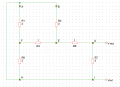
I was hoping someone could point me in the right direction. Attached is a basic digital to analogue converter and my task is to calculate the values for every possible sequence of inputs. I am entirely fine when it comes to calculating the output when there's a single input on the circuit but I'm having trouble with when there is multiple inputs.

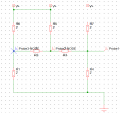
For example, in the attached image inputs A and B are on. I am attempting to simplify the circuit to a purely series or parallel circuit and from there calculating the rest of the values but I am having trouble getting my head around what R2 is doing. I mean, it's not really in parallel or series with anything. It seems to form some sort of triangle with R6 and R5 and I can't figure out the best way to approach it.

Any advise?
 

Attachments

LesJones

Joined Jan 8, 2017
4,174
As you have not labeled the inputs or the output on your diagram I am having to guess. I am assuming this is a normal D to A converter so each input will only have two states. (High or low.) I am guessing that the top end of R7 is an input. If that is so as nothing is connected to the top end of R7 you have introduced a third state for that input which is floating. It is neither high or low. This comment may help your calculations. I have made the following assumptions. It is a three bit D to A converter (So it will have 8 states.) , that the junction of R4 and R7 is the output and the top ends of R5, R6 and R7 are inputs.
Hint. I would use Thevenins theorem to help solve the problem.

Les.
 

Thread Starter

Fnordgasm5

Joined Mar 2, 2013
15
As you have not labeled the inputs or the output on your diagram I am having to guess. I am assuming this is a normal D to A converter so each input will only have two states. (High or low.) I am guessing that the top end of R7 is an input. If that is so as nothing is connected to the top end of R7 you have introduced a third state for that input which is floating. It is neither high or low. This comment may help your calculations. I have made the following assumptions. It is a three bit D to A converter (So it will have 8 states.) , that the junction of R4 and R7 is the output and the top ends of R5, R6 and R7 are inputs.
Hint. I would use Thevenins theorem to help solve the problem.

Les.
Sorry, it made sense to me but then I've been staring at it for hours. Yes, it's a three-bit D to A converter. I've uploaded a better drawing. I've drawn it as if I'm calculating the thevenin equivalent resistance at the Vout terminals.

I could draw it as if I'm calculating the thevenin equivalent voltage but I would still have the same problem. I don't know what to do about R4. It forms kind of a triangle with R1 and R2 and I can't figure out how to simplify that into a series or parallel circuit. Does it simplify or do I have to try something else?
 

Attachments

LesJones

Joined Jan 8, 2017
4,174
You have still not labeled the three inputs. From the circuit as you have drawn it. Starting at the left hand side consider just R1 and R6 which form a potential divider between point H and point A Calculate the voltage at point F with respect to point H. Calculate the source resistance at point F. This is your first Thevenins equivalent point. (Voltage and source resistance.) Next move to the right hand end of R4 by adding in R4 resistance. Then do the Thevenin calculation with the Thevenin equivalent at the right hand end of R4 and R2. Just proceed this way until you get to the output.

Les.
 

dcbingaman

Joined Jun 30, 2021
1,065
Please label the three inputs and label the output. At the moment you are showing two outputs. The schematic without being labeled is very confusing. Of all the junctions, I have no idea which ones are inputs.
 

Thread Starter

Fnordgasm5

Joined Mar 2, 2013
15
Right, so with a little digging I've come to the conclusion that the circuit I am trying to do calculations for is a 3 bit r-2r ladder DAC. You would think that this would be covered in the study materials if I'm expected to submit assignments on them but clearly not.

Anyway, I think I've got a handle on it now. I just need some clarification. From my brief research I can see how to calculate the voltages on a 3 bit DAC and how to use thevenin's to simplify it. Seems easily doable. My question is about the inputs when they are set to "0". On the various web pages I've visited and youtube videos I haven't managed to find a consistent answer. On some it really specify what happens to the inputs when set to "0". They're just floating. And on some they are tied down to the ground point.

Now, I've drawn two circuits and this time I've actually labelled them and not just assumed people will know what they're looking at. One is with the inputs not grounded and the other is with them grounded. The work I've done does heavily suggest the latter but I thought it best to check since I'm making a lot of assumptions.


LesJones

Joined Jan 8, 2017
4,174
When I saw the circuit in the first post I was tempted to re draw it as a r-2r ladder DAC but with R2 and R3 having an unspecified value (Which you corrected in later circuits.) I thought the required answer was in the form of an equation.
As we now know it is a r-2r ladder DAC you know what the output should for each of the 8 input states. So you could do your calculations twice once with an input floating and once with it correctly grounded.
I think the exercise will have also taught you the importance of labeling points on a circuit so others know what they are.

Les.
 

dcbingaman

Joined Jun 30, 2021
1,065
Right, so with a little digging I've come to the conclusion that the circuit I am trying to do calculations for is a 3 bit r-2r ladder DAC. You would think that this would be covered in the study materials if I'm expected to submit assignments on them but clearly not.

Anyway, I think I've got a handle on it now. I just need some clarification. From my brief research I can see how to calculate the voltages on a 3 bit DAC and how to use thevenin's to simplify it. Seems easily doable. My question is about the inputs when they are set to "0". On the various web pages I've visited and youtube videos I haven't managed to find a consistent answer. On some it really specify what happens to the inputs when set to "0". They're just floating. And on some they are tied down to the ground point.

Now, I've drawn two circuits and this time I've actually labelled them and not just assumed people will know what they're looking at. One is with the inputs not grounded and the other is with them grounded. The work I've done does heavily suggest the latter but I thought it best to check since I'm making a lot of assumptions.


Nice, thanks this is much easier to follow. Keep in mind when using superposition, or thevenizing, you short out all voltage sources except the one being analyzed and open all current sources. So yes, when you short the A, B or C you are tying them to ground in this specific circuit. You never open them when performing thevinization/superposition. You always short voltage sources and open current sources.
 
Last edited:

slackguy

Joined Feb 11, 2016
76
I would rather you specify where you are finding this DAC.

Most DAC ADC i see today are complex and support everything short of full MODEM operation. All the inputs and outputs of these are way too complicated for discussion. An analyzer exists and they cost like $40,000 ?

Exactly where are you buying this DAC and for what application? Are there any "3 pole" DAC on the market to find?
 
Top