8 bit Parallel in Serial Out

Thread Starter

spitty19

Joined Apr 5, 2015
11
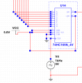
I am trying to create a laser communication system using a 8x8 BJT the BJT is coming from a 3x8 decoder and it working properly, but I have never really worked with a shift register before and am looking for some help and or insight on my situation. I don't know If I am using the correct shift register or not but I have attached an image of what I am working on right now and where I am at.
 

Attachments

MrChips

Joined Oct 2, 2009
30,802
What is an 8x8 BJT?

8-bit shift registers are available.
You have to decide if you want:

serial-in/parallel-out such as 74HC595
or
parallel-in/serial-out such as 74HC165
 

Thread Starter

spitty19

Joined Apr 5, 2015
11
My apologies I thought I said it in my original post I want the parallel in serial out. and what is the difference from those to the SHIFT_8PIN that I am using in my project now as seen in the picture? Like I said I am pretty new to the shift register game haha
 

MaxHeadRoom

Joined Jul 18, 2013
28,684
You could also look at one of the USART/UART IC's, there have been quite a few in the past, I believe the Maxim MAX3100 series will do it.
Max.
 

crutschow

Joined Mar 14, 2008
34,422
A USART/UART, as Max suggested, has built-in synchronism for the transmitter and receiver of the parallel-serial-parallel data at each end, which a standard shift-register does not.
 

Thread Starter

spitty19

Joined Apr 5, 2015
11
is that available in multisim, I guess I should expressed that initially that I am performing everything on multisim until the output from my shift register, id like to stick with the 74HC165 as Mrchips had suggested if possible, as once I get it working in multisim I believe I have some of those readily available
 

MaxHeadRoom

Joined Jul 18, 2013
28,684
Presumably if you have a parallel to serial data transmission, there is some kind of protocol decoding to be done on the receiving end?
Max.
 

Thread Starter

spitty19

Joined Apr 5, 2015
11
Yes that is where the laser communication comes in, im going to use a laser to take the data from the shift register and project it into a photodiode, and then from the photo diode its going to be put into an audio jack and then from the audio jack its going to be brought back into a computer and deciphered using an morse code reader, but I need to figure out how to get the shift register working to be able to do that.
 

MrCarlos

Joined Jan 2, 2010
400
Hello spitty19
And Yes: What is an 8x8 BJT?

The differences between the ones mentioned by MrChips (74HC595 & 74HC165) and the one You are using (SHIFT_8PIN) are similar at the differences between the colors black y white.
You need a IC identification number NOT its name.
never will find, in the market, one SHIFT_8PIN.

So: what is the identification number for your SHIFT_8PIN that you are using in your design ??.

Also: I Can't see the name of the PINS on the picture you have attached.
Could You please do a better job about?

You could use, for your design, the 74HC165, its name is PISO (Parallel IN. Serial OUT). Very similar to your SHIFT_8PIN.
(Attached Data Sheet).

In the future You can find, practically, any data sheet in this link:
http://www.alldatasheet.com/
 

Attachments

Thread Starter

spitty19

Joined Apr 5, 2015
11
an 8x8 BJT ROM its used along with the 3 decoder to produce a desired output based on the 3 bit input your bring into the decoder based on diorthogonal coding.

Nevertheless I have attached another image of my shift register hook up but I know I have it wrong as I am not getting any sort of output on my oscilloscope.
 

Attachments

Thread Starter

spitty19

Joined Apr 5, 2015
11
I understand everything about how it shifts everything along through the shift register I just don't understand how you hook up the CLK, ~CLR, INH, ~SH/LD, SER, and ~QH
 

MrCarlos

Joined Jan 2, 2010
400
Hello spitty19

Let me tell you a much of things:
The 74HC165 has both characteristics: PISO & SISO.
You are trying to use It as PISO, Parallel-IN, Serial-OUT.

In order to use that way you must:
Load the parallel data in the internal registers.
- Setup the data in all the D's inputs.
- Apply a negative transition pulse at PIN 1 (Shift/Load'). This PIN in standby must be High.
- Make false the PIN 15 (Inhibit). Low.
- Apply 8 positive transition pulses at PIN 2 (Clock).

All data on the D inputs should appear in its output QH(9).
The PIN 7 is only the complement of PIN 9.
 

MrCarlos

Joined Jan 2, 2010
400
Hello spitty19

Well, You can use a Switch or one button or a signal coming from x.

I think You are missing something: The receiving end must know that Data are arriving. This means "To synchronize".

Let me call, to the data You are sending as: string.
How, the receiving end, knows, that a string of data is arriving ?.
How determine the beginning and the end of such string.
Should exist something named Protocol.
- hey, I am going to send some data.
- Ok send me those, I ready to receive.
- Well, Going there.
- Have received 8 BITs, it is ok?
- Yes.

Let us see your full project, if possible, in order no guessing.
 

MrCarlos

Joined Jan 2, 2010
400
Hello spitty19
keep in view the attached document.
Because You are novice:
Let's talk a little about the 74LS165 Parallel-in/serial-out 8-Bit Shift Register.

As You can see by it's symbol, it has 8 Data BIT's inputs, D0(11), D1(12), D2(13), D3(14), D4(3), D5(4), D6(5), D7(6).
Through those PIN’s You program the data to be send.
Note, also, that this IC has another PIN SI(10); with this make its function SISO(Serial-IN/Serial-OUT).
Now: The PIN named SH/LD'(1) has double Function:
LD' Load the data on its PIN’s Dx(x) into its internal registers. True: LOW level.
SH Shift The data in its internal registers. True: HIGH level.
CLK(2) At each positive transition of the pulse applied to this PIN, the data in the internal registers will be Shifted, and will be appearing at its output SO(9).
Furthermore the input named INH(15) INHibit, precisely, the full Function of this IC. True: HIGH level.

Now The outputs:
It has two: SO(9) and QH'(7).
Through SO(9), The Data entered by Dx(x) or SI(19) Inputs, will coming out serially.
One after the other.
As I mentioned earlier QH'(7) is just the complement of the logic state of S0(9).

The numbers in parentheses indicate PIN number.
All this wording are in the data sheet in message #9. And More.
Have You studied those data sheets?.

In order to practice, you can assemble the circuit appearing in the attached document in Your Multisim simulator. Play with it by a while.

I Hope that helps a bit.
 

Attachments

Thread Starter

spitty19

Joined Apr 5, 2015
11
Sorry for the delay , but this is the 8 bit that I was to bring into the shift register and portray out the serial data. As I had said the btw is working correctly and I have the laser part working correctly, I just need to finish it with the shift register.
 

Attachments

Top