 Facebook
 Google
 GitHub
 Linkedin
Hello all. So I'm an engineering technician who typically doesn't deal with circuits on this code of a level, but a passion of mine has me recently diving deep into old school IC chips in great detail. That passion would be the Redstone creations using the video game Minecraft.
Do to the heart of the matter.
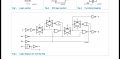
The attached picture is of a 74HCT74 chip. I understand the use of this chip but as I'm trying to create the blocky logic gates I came across the weird mid section of this chip. Can someone explain to me what exactly and how the portion that looks like 2 inverters pointing into each other with 2 buffers pointing each other works? Because with my understanding of this circuit I'm seriously confused how an inverter or buffer would output into a line that had a clock pulse inputting into that line as well. In a dc circuit it would basically look like 3 lines merging into a point with no where to go.
See. I'm seriously confused. Lol
Any and all help would be greatly appreciated.
Sincerely,
ZomBoSk8r
Do to the heart of the matter.
The attached picture is of a 74HCT74 chip. I understand the use of this chip but as I'm trying to create the blocky logic gates I came across the weird mid section of this chip. Can someone explain to me what exactly and how the portion that looks like 2 inverters pointing into each other with 2 buffers pointing each other works? Because with my understanding of this circuit I'm seriously confused how an inverter or buffer would output into a line that had a clock pulse inputting into that line as well. In a dc circuit it would basically look like 3 lines merging into a point with no where to go.
See. I'm seriously confused. Lol
Any and all help would be greatly appreciated.
Sincerely,
ZomBoSk8r
Attachments
-
 139.1 KB Views: 29


