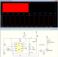
555 Timer Output dip after MOSFET driving in LT spice Simulation

Thread Starter

mishra87

Joined Jan 17, 2016
1,037
Hi All,

Can anyone figure out why 555 timer output is not coming as per expected ?
The output should be 10V peak to peak but it is getting loaded with mosfet gate charge.

I want to drive dc motor rated 18V @ 15A.
The idea here to give motor soft start using PWM signal with minimum duty cycle with frequency e.g. 6.8KHz, 16KHz.
I want to give motor soft start for 1 sec before running with 100% duty cycle.
I was trying to implement using discrete components, may be i also need some circuit to drive mosfet for after 1sec with 10V dc not pwm.

Any recommendation on the same is highly appreciable.

Thanks !!

1633104479943.png
1633104521202.png
1633105503139.png
 

Attachments

bertus

Joined Apr 5, 2008
22,277
Hello,

Could it be that R3 is to large?
The supply is 18 Volts and the zener 10 Volts, so there is a current of 8 mA available.
The zener will need some of the current for the correct working.

Bertus
 

ericgibbs

Joined Jan 29, 2010
18,849
I have doubts if this circuit works for motor driving for 15amps and 470uF cap is to high and not available in ceramic smt.
hi,
In that case you will have to create a suitable 10V supply for the project.
The 470uF is not ceramic, it is electrolytic.

What is the Drain load on the MOSFET,? that requires 15Amps.?
E
 

crutschow

Joined Mar 14, 2008
34,452
Here's the circuit modified to give the desired 1 second low duty-cycle startup and then going to 100% duty-cycle.
R3 was starving the circuit so I reduced its value and added C2 filter.
Also increased the value of R5, since that has no effect on the waveform to the MOSFET gate.
You don't need D4.
I didn't have models for some of your parts, so I used ones I had.
You may have to tweak the values of R6 and/or C3 to get the desired startup time due to the wide tolerance of M2's gate threshold voltage.

1633111709218.png
 

Thread Starter

mishra87

Joined Jan 17, 2016
1,037
hi,
In that case you will have to create a suitable 10V supply for the project.
The 470uF is not ceramic, it is electrolytic.

What is the Drain load on the MOSFET,? that requires 15Amps.?
E
Hi E,

Thanks for reply !
Drain load is DC motor .

Regards,
 

Thread Starter

mishra87

Joined Jan 17, 2016
1,037
Here's the circuit modified to give the desired 1 second low duty-cycle startup and then going to 100% duty-cycle.
R3 was starving the circuit so I reduced its value and added C2 filter.
Also increased the value of R5, since that has no effect on the waveform to the MOSFET gate.
You don't need D4.
I didn't have models for some of your parts, so I used ones I had.
You may have to tweak the values of R6 and/or C3 to get the desired startup time due to the wide tolerance of M2's gate threshold voltage.

View attachment 249224
Hello C,

Thank you very much !
That is what I was looking for.

if do not mind, could you please explain the purpose of additional circuit (m2, r6, c3). How this RC generating pulse for 1 sec and then it becomes high after 1 sec.

thanks again !
 

crutschow

Joined Mar 14, 2008
34,452
could you please explain the purpose of additional circuit (m2, r6, c3).
When power is applied the M2's gate voltage is 0V and the transistor is off, allowing the 555 timer to generate the desired start pulses.
When C3 charges to the gate threshold voltage through R6 after about 1s due to the R6C3 time-constant, M2 turns on.
This pulls the TRIG and THRS voltage to ground, triggering the 555 timer to OUT high.
Since C1 is now prevented from charging, the THRS trigger turn-off voltage is never reached and the OUT stays high until the power is removed.

If you don't know, the 555 is basically a level-triggered latch.
A low on the TRIG input (triggers at 1/3 Vcc) sets the OUT high, and a high on the THRS input (triggers a 2/3 Vcc) sets the OUT low.
DIS discharges C1 when the OUT is low.
 

LowQCab

Joined Nov 6, 2012
4,072
The Zener-Diode across the Motor is probably already smoked.

Use an Ultra-High-Speed Diode rated for the full start-up-Current of the Motor.

The Motor needs the Diode to recirculate the Voltage generated by the
collapsing Magnetic-Field which occurs every time the FET switches Off.
Otherwise, ~10% Duty-Cycle may not be enough to
actually get the Motor up to speed.

A much, much, much lower frequency would work better, maybe ~100hz or so.

Smoothly ramping the Duty-Cycle from 0 to 100% would be a better plan,
but would require a slightly more complex Circuit using
an Op-Amp instead of a 555.
.
.
.
 

Thread Starter

mishra87

Joined Jan 17, 2016
1,037
The Zener-Diode across the Motor is probably already smoked.

Use an Ultra-High-Speed Diode rated for the full start-up-Current of the Motor.

The Motor needs the Diode to recirculate the Voltage generated by the
collapsing Magnetic-Field which occurs every time the FET switches Off.
Otherwise, ~10% Duty-Cycle may not be enough to
actually get the Motor up to speed.

A much, much, much lower frequency would work better, maybe ~100hz or so.

Smoothly ramping the Duty-Cycle from 0 to 100% would be a better plan,
but would require a slightly more complex Circuit using
an Op-Amp instead of a 555.
.
.
.
Hello,
Thanks for your discussion !
How will you use opamp to ramp up the duty cycle from 0% to 100% ?

Regards,
M
 

crutschow

Joined Mar 14, 2008
34,452
How will you use opamp to ramp up the duty cycle from 0% to 100% ?
Below is a circuit that uses not an opamp, but an LM339/LM393 comparator PWM circuit to ramp the PWM duty-cycle from 0 to 100% duty-cycle, as LQC suggested, (in about 1.35s as determined by R7-C2) after circuit power is applied.
The PWM frequency is about 106Hz as determined by the R1-C1 values shown.
V(out) low indicates full voltage applied to the motor.

1633140692558.png
 
Last edited:

Thread Starter

mishra87

Joined Jan 17, 2016
1,037
Below is a circuit that uses not an opamp, but an LM339/LM393 comparator PWM circuit to ramp the PWM duty-cycle from 0 to 100% duty-cycle, as LQC suggested, (in about 1.35s as determined by R7-C2) after circuit power is applied.
The PWM frequency is about 106Hz as determined by the R1-C1 values shown.
V(out) low indicates full voltage applied to the motor.

View attachment 249271
Hello C,

Thank you so much for support !
Unfortunately my simulation did not work. I did not have LM339 model with me so i used LT1017 with open collector output (file attached)
Could you please attached your simulation file ?

As per my understanding :
1. U1a is working as a free running multivibrator.
What is use of R5 here ?
2. U1b is used as comparator and output of U1b by default is high so during the turn on M1 gets turned ON.
what is the use of R8 and R10 here ?
How this will generate the pulse for 1.35s.
What is use of D1 ?

I would suggest M1 should see low during turned ON.

Could you please help me to understand a bit better of this circuit ?
1633161673928.png
 

Attachments

crutschow

Joined Mar 14, 2008
34,452
What is use of R5 here ?
That, along with R2 and R3, establish the upper and lower trip voltages for the multivibrator at 1/3 and 2/3 of V+.
what is the use of R8 and R10 here ?
Generates a start voltage for C2 of about 6V so there is no delay for the pulse output startup.
If C2 is connected to ground, there is about a 0.8s delay before the output starts.
If that's not a problem, then you can eliminate R8 and R10, and connect C2 to ground.
How this will generate the pulse for 1.35s.
It doesn't.
It's the charging of C2 by R7 that determines the delay time (as I previously stated).
When the voltage on C2 goes about the upper triangle voltage of 12V, the PWM pulses stop and the comparator output stays high.
I would suggest M1 should see low during turned ON.
I don't see that single pulse as a problem, but moving the C1 connection from ground to V+. as Bordodynov suggested, eliminates that.
What is use of D1 ?
Discharges C3 rapidly when the power is removed and prevents C3 from dumping a large spike current into the comparator input, which could damage it.
Could you please help me to understand a bit better of this circuit
U1a generates a 6v-12V triangle-wave (TRI).
U1b's output goes high when the Mod_In voltage is higher than the triangle-wave voltage.
Since the Mod_In voltage is increasing due to the charging of C3, U1b's trigger point on the triangle-wave is changing, causing the output pulse width to also change with time, giving the change in its duty-cycle.
Make sense?
Unfortunately my simulation did not work.
It didn't work because you need to start the simulation without doing the initial DC analysis, which sets the value of C3 at 18V.
Use the uic option in the simulation command.
1633184856934.png

File attached.
 

Attachments

Last edited:

Thread Starter

mishra87

Joined Jan 17, 2016
1,037
That, along with R2 and R3, establish the upper and lower trip voltages for the multivibrator at 1/3 and 2/3 of V+.
Generates a start voltage for C2 of about 6V so there is no delay for the pulse output startup.
If C2 is connected to ground, there is about a 0.8s delay before the output starts.
If that's not a problem, then you can eliminate R8 and R10, and connect C2 to ground.
It doesn't.
It's the charging of C2 by R7 that determines the delay time (as I previously stated).
When the voltage on C2 goes about the upper triangle voltage of 12V, the PWM pulses stop and the comparator output stays high.
I don't see that single pulse as a problem, but moving the C1 connection from ground to V+. as Bordodynov suggested, eliminates that.
Discharges C3 rapidly when the power is removed and prevents C3 from dumping a large spike current into the comparator input, which could damage it.
U1a generates a 6v-12V triangle-wave (TRI).
U1b's output goes high when the Mod_In voltage is higher than the triangle-wave voltage.
Since the Mod_In voltage is increasing due to the charging of C3, U1b's trigger point on the triangle-wave is changing, causing the output pulse width to also change with time, giving the change in its duty-cycle.
Make sense?
It didn't work because you need to start the simulation without doing the initial DC analysis, which sets the value of C3 at 18V.
Use the uic option in the simulation command.
View attachment 249314

File attached.
Hello C,

Thank you very much for support !
It was a great learning for me.

Best wishes,
 

Thread Starter

mishra87

Joined Jan 17, 2016
1,037
That, along with R2 and R3, establish the upper and lower trip voltages for the multivibrator at 1/3 and 2/3 of V+.
Generates a start voltage for C2 of about 6V so there is no delay for the pulse output startup.
If C2 is connected to ground, there is about a 0.8s delay before the output starts.
If that's not a problem, then you can eliminate R8 and R10, and connect C2 to ground.
It doesn't.
It's the charging of C2 by R7 that determines the delay time (as I previously stated).
When the voltage on C2 goes about the upper triangle voltage of 12V, the PWM pulses stop and the comparator output stays high.
I don't see that single pulse as a problem, but moving the C1 connection from ground to V+. as Bordodynov suggested, eliminates that.
Discharges C3 rapidly when the power is removed and prevents C3 from dumping a large spike current into the comparator input, which could damage it.
U1a generates a 6v-12V triangle-wave (TRI).
U1b's output goes high when the Mod_In voltage is higher than the triangle-wave voltage.
Since the Mod_In voltage is increasing due to the charging of C3, U1b's trigger point on the triangle-wave is changing, causing the output pulse width to also change with time, giving the change in its duty-cycle.
Make sense?
It didn't work because you need to start the simulation without doing the initial DC analysis, which sets the value of C3 at 18V.
Use the uic option in the simulation command.
View attachment 249314

File attached.
Hello Again,

Did anyone figure out the problem in the circuit ?
LM339 can source max 20mA current per datasheet.
Lets say Qg of Mosfet is 50nC, Duty 10% of 16KHz so peak current of mos gate will be 70mA (not exact calculated).
So there will problem in mos switching .

May be we have add some circuit.

Thanks
 
Top