23LC1024 RAM

Thread Starter

q12x

Joined Sep 25, 2015
1,690
Hello again with another small project.
I followed this video tutorial and I also buy that 23LC1024 IC RAM she is presenting (5pcs from aliexpress under 10$)
She(the instructor) is providing the arduino project file is using in a link in the video description. - that is what I used.
Here is my implementation in reality. And it worked !
IMG_20220908_230217.jpg
Here is my implementation in proteus simulator. And it worked as well !
1662669828640.png
So double victory so far.
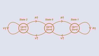
All good and well, but.... I need and want to understand this more in depth.
Of course I will experiment by myself, but in parallel, some interesting and good advice from this forum will be of much help to me.
Just put your ideas, your thoughts, down on the table, about how to manually or more logically get or set data into this RAM. Speculations are fine, but if you happen to know more precise about how to use a RAM chip like this, is awesome. But your wild guess is as much help to me as well. I understand this is a bit high level and not that common use, at least in my eyes .
This probably will be more programming than electronics. Since all the hardware is already deal with. Additional hardware is interesting to see what you can come with, again, ideas, something cool. I believe a processor unit will be necessary to actually R/W to the RAM chip. I guess..... Hmmm.
She(the instructor) in the title of the video clearly say this RAM is "Extending Arduino Uno RAM".... I may be mistaken buying it and all that code to be very specific linked to arduino uno ---extension--- ? In my mind, this is a practice chip to learn more in depth about this side of technology. I hope I can jump out of the line that she is presenting and actually do whatever I want with this chip. I hope im right.
Thank you and I wait your answers !
---
Ps: I put this arduino project test file here in the attachment for posterity.
(this file is from the tutorial, NOT made by me, so all credits goes to this very well informed and helpful instructor)
 

Attachments

Last edited:

Thread Starter

q12x

Joined Sep 25, 2015
1,690
What are you asking?
my friend @boostbuck , like I said: "... how to manually or more logically get or set data into this sRAM ? ... "
Like I did it with the EPROM, logically and distinctively sending bits to each address.
I want this here as well. I want something that resembles with a beginner tutorial on how to R/W to this SRAM. Or plain explanation, discuttion maybe, if no easy tutorials exist.
I am right now reading this sram wiki page, and they are clearing up a good bunch of fog about this SRAM, where and how is used. Also half of the page lecture is about how is built and it's internal mechanics. Yah, I read it now, after I buy the thing, haha. But my good sense never failed me. I still believe is a very important component. For my future projects. It better be, haha.
 

Thread Starter

q12x

Joined Sep 25, 2015
1,690
I believe the key word that describe the best what Im searching for is:
- Manual programming an SRAM -
(and the good news is that I can test it in both: reality and simulator)
 

boostbuck

Joined Oct 5, 2017
515
The datasheet gives very explicit instructions for programming the interface. I doubt that I could do much more than recommend you follow the instructions there. If you code the behaviours specified you should succeed in reading and writing.
 

Thread Starter

q12x

Joined Sep 25, 2015
1,690
The datasheet gives very explicit instructions for programming the interface. I doubt that I could do much more than recommend you follow the instructions there. If you code the behaviours specified you should succeed in reading and writing.
Yah, I looked into its datasheet already and I believe I figure out its mechanism. I hope im right.
Im still curious what you believe its mechanism may be?
Share your thoughts.
 
Last edited:

dl324

Joined Mar 30, 2015
16,918
how to manually or more logically get or set data into this sRAM ? ... "
Like I did it with the EPROM, logically and distinctively sending bits to each address.
It sounds like you don't want a serial device. Look at devices like 6116.

Or more interesting devices like X2110 (NVRAM). They didn't make these in high capacity... For that, you'd use EEPROM or NOR FLASH.
 

Attachments

Thread Starter

q12x

Joined Sep 25, 2015
1,690
How do I make a logic counter with 7493 that goes OVER 16 beats ?
(I need 24 beats to be more specific) I know I have to link 2x7493 but I don't know how exactly.
Provide me a quick circuit please.
Thank you.
1662769695325.png
 

Jony130

Joined Feb 17, 2009
5,488
And now, how I specifically make it count to 24?
But this circuit already is counting to 24.
24 in binary is 11000 and this state (11) is "detected" by AND gate. And the gate reset the counter. Thus, the counter will start counting from zero.

Did you set the "VSM Counter Timer" into frequency meter mode? Because 100kHz/24 = 4166Hz

Or you could try this version
7493_mod12b.PNG

F_out =24kHZ/24 = 1000Hz
 
Last edited:

Thread Starter

q12x

Joined Sep 25, 2015
1,690
oooh, I didnt stay to watch until it ends actually. My mistake entirely. I leave it for a couple of seconds and I presume it was going to infinite. Daaaeeem.
- Ok so to be more clear, I mentioned that I need 24 "beats" this means at the rate of 1Hz, this means 1 beat per 1 second, if I count 24 seconds, it will beat 1 time per 1 second and it will be 24 beats until the end of the cycle. And when it gets to 24, it resets back to 0 and start again. Very simplistic logic. Not binary fancy. This is pure decimal fancy.
 

Jony130

Joined Feb 17, 2009
5,488
So you want to have a high state at the output for 24 clocks "beats" and a low state for 24 clocks "beats" and start again?
 

Thread Starter

q12x

Joined Sep 25, 2015
1,690
No.
1 beat = 1High AND 1Low. So theoretically are 48 'steps' for each high and low, but I count as a 'beat' only the High, while the Low is automatically included.
For example: In this small image I make, there are 4 beats, of High and Low. But if you count the actual 'steps' there are 8 steps, one step for each High OR Low.
1662881756567.png
 

Thread Starter

q12x

Joined Sep 25, 2015
1,690
- I believe you understand very well what Im saying.
- I will give you an assignment: Count to 3 using a 7493 IC. Find a way to count to this number. 1 single chip can count to 16 as it's maximum. So I give you the simplest one possible.
- I will give you the written answer how to make it though: CKB is always linked to QA. You apply a pulse to CKA. R01 is linked to QA and R02 to QB. You will have to add a NAND gate on R01 and R02 from which a FlipFlop will be Cloked and from it's Q (not /Q) a LED to the gnd is linked. This is the entire circuit. Now you can build it following these instructions.
 

Thread Starter

q12x

Joined Sep 25, 2015
1,690
I tried these days to find a solution on figuring out a way of writing this sram chip. And no success. I went to arduino forums, on other electronic forum and they practically move their shoulders up and down. I tried a lot of codes but with no success. Im very sad about it. It will remain to be solved in the future perhaps.
 

Thread Starter

q12x

Joined Sep 25, 2015
1,690
As I said, I discussed these problems in other forums. I will post the highlights from them:
----
Here are two diagrams from the datasheet that I used all the time while coding:
1663260216379.png
and
1663260228369.png
With help from the Arduino forums, I advanced to a point where I get a result, but is not the correct result.
What I am doing in this code: I am directly accessing the pins of the RAM, by a method called 'Bit Banging'. I am hardcoding the instructions, and sending them manually as simply as possible.
The result is still incorrect. Please, advise me where the problem is that I can't see?
This is the output console from the Proteus simulator. The transmitted bits should be the same in the received/read bits. I am clearly missing something, but what?
1663260260041.png
The folowing is the Arduino code:
C++:
#include "Arduino.h"

/************SRAM opcodes: commands to the 23LC1024 memory chip ******************/

#define clk        13 // Manual Serial Clock
#define wpin       12 // Write pin
#define rpin       11 // Read pin
#define cspin      10 // Chip Select

/************Global Variables*********************/

byte bcode = 0b11100111; // test bitcode to send/receive only once

void setup(void) {
  Serial.begin(9600);

  pinMode(clk, OUTPUT);
  pinMode(wpin, OUTPUT);
  pinMode(rpin, OUTPUT);
  pinMode(cspin, OUTPUT);
  digitalWrite(cspin,LOW); // ChipSelect CS is Low to start and High to end a read/write operation.
  digitalWrite(rpin,LOW); // initialize read pin as Output Low

  /*
  --------------------------
  ---------Writing----------
  --------------------------
  */
  digitalWrite(cspin, LOW); // starting write operation
  Serial.println("Transmiting data:");
  digitalWrite(clk, 0);

  //-------------1st: 8bit initialization-------------
  //this is 00000010
  for (int i = 0; i < 6; i++) {
    digitalWrite(clk, 1);
    digitalWrite(wpin, 0); // only 6 0's
    digitalWrite(clk, 0);
  }
  digitalWrite(clk, 1);
  digitalWrite(wpin, 1); // 7th bit
  digitalWrite(clk, 0);
  digitalWrite(clk, 1);
  digitalWrite(wpin, 0); // 8th bit
  digitalWrite(clk, 0);

  //-------------2nd: 24bit address-------------------
  //this is 00000000 00000000 00000001
  for (int i = 0; i < 23; i++) {
    digitalWrite(clk, 1);
    digitalWrite(wpin, 0); // last 23 addr bits
    digitalWrite(clk, 0);
  }
  digitalWrite(clk, 1);
  digitalWrite(wpin, 1); // first 1 addr bit (reading from R to L)
  digitalWrite(clk, 0);

  //-------------3rd 8bit code-----------------------
  digitalWrite(clk, 1);
  digitalWrite(wpin, bcode); // WRITE bitcode into RAM address
  Serial.println(bcode, BIN);
  digitalWrite(clk, 0);

//CSpin
digitalWrite(clk, 1);
// from datasheet: "A write is terminated by the CS being brought high"
digitalWrite(cspin,HIGH); // finishing write operation
digitalWrite(clk, 0);
digitalWrite(clk, 1);
digitalWrite(cspin,LOW); // starting read operation
digitalWrite(clk, 0);

  /*
  --------------------------
  ---------Reading----------
  --------------------------
  */
  Serial.println("Receiving data:");

  //-------------1st: 8bit initialization-------------
  // this is 00000011
  for (int i = 0; i < 6; i++) {
    digitalWrite(clk, 1);
    digitalWrite(wpin, 0); // only 6 0's
    digitalWrite(clk, 0);
  }
  digitalWrite(clk, 1);
  digitalWrite(wpin, 1); // 7th bit
  digitalWrite(clk, 0);
  digitalWrite(clk, 1);
  digitalWrite(wpin, 1); // 8th bit
  digitalWrite(clk, 0);

  //-------------2nd: 24bit address-------------------
  //this is 00000000 00000000 00000001
  for (int i = 0; i < 23; i++) {
    digitalWrite(clk, 1);
    digitalWrite(wpin, 0); // last 23 addr bits
    digitalWrite(clk, 0);
  }
  digitalWrite(clk, 1);
  digitalWrite(wpin, 1); // first 1 addr bit (reading from R to L)
  digitalWrite(clk, 0);

  //-------------3rd 8bit code-----------------------
  //this should be 11100111
  byte result = 0;
  String strout="";
  for (int i = 0; i < 8; i++) {
    digitalWrite(clk, 1);
    // In SDI mode, the transfer is two bits per clock pulse.
    strout+=bitRead(rpin, i); // is giving me 11010000 instead of 11100111
    digitalWrite(clk, 0);
  }
  Serial.println(strout); // READ bitcode into RAM address
  digitalWrite(cspin, HIGH); // finishing read operation
}

void loop() { // we have nothing to do in the loop
}

//End of program
The summary of my code is very simple: I write this hardcoded : "byte bcode = 0b11100111; " that I am sending to be written into the chip at address 000...0001 (24bits long address) and then I am reading the chip output pin again at the same address and retrieve the data stored at that address. But instead of being 11100111 (this lovely test pattern), is something else. Is this result that appears, doesnt matter what input pattern I insert: 1663260375897.png
The guys from arduino forums introduced me to bit banging and I have a pretty good idea what it is. I am not that advanced into SPI comunication though, but I also got the idea.
Its this chip... you see? It has some very special way of communicating even if is SPI. Its from Microchip and they always had to add some weird way of access, indifferent of the component they sell. But after figuring out the little details and make it work, then is a very reliable component.
All I need is NOT to comunicate through a standard SPI way, but through bitbanging, simulating a SPI comunication. Thats my intention.
I strongly believe is not a matter of arduino anymore. Because the guys there would have spotted already any mistake. We are banging this code for a few days already. I believe is a matter of microchip mischievousness in sending/receiving that entire instruction. It is my conclusion after staring too much into this problem.

I also find this little detail that I have no idea how to implement it. But it is exactly the same result that I keep getting in the output 1663260516189.png , indiferent what input test bitcode I send:

I put an attachment here ( 23LC1024.zip )with the arduino code, the proteus save file and the circuit diagram.
Thank you !
 

Attachments

Jony130

Joined Feb 17, 2009
5,488
Her you have I fix your circuit and the code.

The circuit:

SPI_12.PNG


C++:
/************SRAM opcodes: commands to the 23LC1024 memory chip ******************/
#define clk        13       // Manual Serial Clock
#define wpin       12       // Write pin
#define rpin       11       // Read pin
#define cspin      10       // Chip Select
/************Global Variables*********************/
byte bcode = 0b11100111;   //test bitcode to send/receive only once
byte cnt = 0x80 ; // Bit_Mask
byte result = 0;

void setup(void) {
Serial.begin(9600);

pinMode(clk, OUTPUT);
pinMode(wpin, OUTPUT);
pinMode(rpin, INPUT_PULLUP);
pinMode(cspin, OUTPUT);
digitalWrite(cspin,LOW);  //ChipSelect CS is Low to start and High to end a read/write operation.
/*
--------------------------
---------Writing----------
--------------------------
*/
digitalWrite(cspin,LOW);      //starting write operation
Serial.println("Transmiting data:");
digitalWrite(clk, 0);
delay(1);

//-------------1st: 8bit initialization-------------
//this is 00000010
  for(int i = 0; i < 6; i++)
  {
    digitalWrite(wpin, 0);  //only 6 0's
    delay(1);
    digitalWrite(clk, 1);
    delay(1);
    digitalWrite(clk, 0);
    delay(1);
  }
  digitalWrite(wpin, 1);
    delay(1);
  digitalWrite(clk, 1);
  delay(1);             //7th bit
  digitalWrite(clk, 0);
  delay(1);
  digitalWrite(wpin, 0); //8th bi
  delay(1);
  digitalWrite(clk, 1);
  delay(1);
  digitalWrite(clk, 0);
  delay(10);


//-------------2nd: 24bit address-------------------
//this is 00000000 00000000 00000001
  for(int i = 0; i < 23; i++)
  {
    digitalWrite(wpin, 0); //last 23 addr bits
    delay(1);
    digitalWrite(clk, 1);
    delay(1);
    digitalWrite(clk, 0);
    delay(1);
  }
  digitalWrite(wpin, 1); //first 1 addr bit (reading from R to L)
  delay(1);
  digitalWrite(clk, 1);
  delay(1);
  digitalWrite(clk, 0);
  delay(10);
//------------------------------------------
digitalWrite(wpin, 0);
//-------------Data Byte-----------------------
Serial.println(bcode, BIN);

while (cnt){
  if (bcode & cnt) digitalWrite(wpin, 1);
  else digitalWrite(wpin, 0);
  delay(1);
  digitalWrite(clk, 1);
  delay(1);
  digitalWrite(clk, 0);
  cnt >>= 1;
}
  digitalWrite(wpin, 0);
  digitalWrite(cspin,HIGH);    //finishing write operation


///*
//--------------------------
//---------Reading----------
//--------------------------
//*/
Serial.println("Receiving data:");

digitalWrite(cspin,LOW);
delay(1);
//-------------1st: 8bit initialization-------------
//this is 00000011
  for(int i = 0; i < 6; i++)
  {
    digitalWrite(wpin, 0);   //only 6 0's
    delay(1);
    digitalWrite(clk, 1);
    delay(1);
    digitalWrite(clk, 0);
    delay(1);
  }

  digitalWrite(wpin, 1);//7th bit
  delay(1);
  digitalWrite(clk, 1);
  delay(1);
  digitalWrite(clk, 0);
  delay(1);
  digitalWrite(wpin, 1); //8th bit
  delay(1);
  digitalWrite(clk, 1);
  delay(1);
  digitalWrite(clk, 0);
  delay(1);


//-------------2nd: 24bit address-------------------
//this is 00000000 00000000 00000001
   for(int i = 0; i < 23; i++)
  {
    digitalWrite(wpin, 0); //last 23 addr bits
    delay(1);
    digitalWrite(clk, 1);
    delay(1);
    digitalWrite(clk, 0);
    delay(1);
  }
  digitalWrite(wpin, 1); //first 1 addr bit (reading from R to L)
  delay(1);
  digitalWrite(clk, 1);
  delay(1);
  digitalWrite(clk, 0);
  delay(10);
///------------------------
digitalWrite(wpin, 0);
//-------------3rd 8bit code-----------------------
//this should be 11100111
  for(int i = 0; i < 8; i++)
  {
    digitalWrite(clk, 1);
    delay(1);
   if( digitalRead(rpin) == HIGH ) result |= ( 1 << (7 - i)); // Set the bit if SO pin HIGH
   else result &= ~( 1 << (7 - i) );                            // Clear the bit if SO pin LOW
    digitalWrite(clk, 0);
    delay(1);
  }
  Serial.println(result,BIN);     //READ bitcode into RAM address

  digitalWrite(cspin,HIGH);   //finishing read operation
  delay(1);
}
                  
void loop() {
}
You must remember that you need to first set (output) the "data" at the falling edge (at low state) of a CLK and then you apply the positive edge CLK.
 

Attachments

Last edited:

Thread Starter

q12x

Joined Sep 25, 2015
1,690
Her you have I fix your circuit and the code.
In the beginning I thought you are joking, but you really did it.
Fantastic man, absolutely fantastic. The use of the osciloscope is purely genius ! I didnt think on using it for a bit ! What a mistake from my part and what a lesson I get from you. I have no words. You are the man, truly. I am very happy now.
And I also looked on your code. I am good but not THAT good Im always saying, but you are THAT good !!! Haha. Oau... the use of that bit mask... I wouldnt think to use it in a milion years. I never knew existed in the first place. Some high end code there. My hat off.
Thank you very - very much mister @Jony130 !
 
Last edited:
Top