USB cable switch

Thread Starter

rsfoto

Joined May 14, 2013
134
Hi,

I am starting a new thread with my USB cable switch project because now I need help for making the PCB. I would just need the Gerber or whatever name the files are called as I have a company here in Mexico who makes boards but the minimum amount are ten of this boards.

For ten PCBs sized 2cm x 6cm they charge about GBP 120.00 but they also need the Gerber¿? files.

Maybe shipping from somewhere else in the world makes it cheaper. As the price depends of the PCB board size I could see if making outside of Mexico is cheaper then buying ten boards here in Mexico.

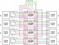
I am willing to pay for the job as it will involve expertise from the person who will help me because my idea is to place 4 or 8 of the circuits on a pcb with the chosen parts or even choosing other parts in order to make it as compact but safe as possible in regard to RF interference.

For example instead of using 8 TLP521-1 I can use 2 TLP521-4 or maybe even smaller SMD devices from a different brand which make the same function. I would like todiscuss this too.

Maybe making single small PCBs is also a better idea. I already found a company which makes metallic mesh and I am already talking to them.

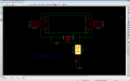
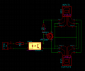
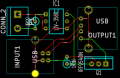
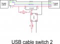
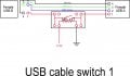
Below you can see the electronic circuit which I did draw with my CAD Program and so far I think I will need a 2 layer PCB in order to accomodate the devices in a row.

I have read about Robin Mitchell but he needs already files from Eagle or KiCad but so far I am not able to make these files as I still have not yet understood how the programs work. :confused:

Thanks for your Interest.
 

Attachments

Last edited:

Thread Starter

rsfoto

Joined May 14, 2013
134
Playing around a bit with KiCad this is as far as I have got.

See attached image.

Now the problem is how to create the board. Especially in regard to the 2 USB connector which have a different footprint as well as the MOSFET and the Optocoupler ¿?

Thanks for any tips.
 

Attachments

Thread Starter

rsfoto

Joined May 14, 2013
134
UPDATE

:)

Looks like I am a step forward with KiCad as I was abke to create files with the endings

*.cmp ; *.net ; *.sch

but I have not found a 4 pin footprint for the TLP 521-1

I looked at all footprints in the PDF sheet but found any which looks like a 4 feet DIP socket and so I used a 6 pin but the connections are wrong ¿?

Another problem is the MOSFET foorprint. It was noct connected at all or do I not see them because they are in some other layer ? I used the TO220GDS footprint.

Anybody can help ? Thanks :)
 
Last edited:

Thread Starter

rsfoto

Joined May 14, 2013
134
youll probably have to make your own part.
Hi,

Thanks. Well I did take a close look into the PDF files again and found a so called PIN_ARRAY_2X2 and that did take care of my problem.

But now working on trying to make a PCB layout I still have the problem when running the ERC test that I have a few conenction errors but everything is connected according to me.

Also when reading the netlist I get the error that the pads 1,2 and 3 for the MOSFET connections are not found.

Could anybody help me with this.

I have attached my *.sch file. What other files do I have to upload so somebody can check it ?

Thanks
 

Attachments

ErnieM

Joined Apr 24, 2011
8,377
Some "simple" devices like MOSFETs have so many package styles they may pop up in it is not uncommon to make a schematic symbol without any pin numbers.

This way an error is guaranteed to appear, and give the designer a chance to fix it with the correct pin numbers for the functions.

When sharing the schematic file also share any custom libraries you made. I opened your schematic, but the MOSFET didn't load as I don't have the library you used.
 

ErnieM

Joined Apr 24, 2011
8,377
BTW, I get small boards made in china for under 30GBP (25 USD), yours would be more but not more then twice.

I found my vendors on EBay.
 

Thread Starter

rsfoto

Joined May 14, 2013
134
Some "simple" devices like MOSFETs have so many package styles they may pop up in it is not uncommon to make a schematic symbol without any pin numbers.

This way an error is guaranteed to appear, and give the designer a chance to fix it with the correct pin numbers for the functions.

When sharing the schematic file also share any custom libraries you made. I opened your schematic, but the MOSFET didn't load as I don't have the library you used.
Hi,

Thanks. Well I used as MOSFET the IRF9540N which is a P channel MOSFET too and just renamed it. After a bit of more experimenting I changed the footprint from TOS220GDS just to TOS220 and the pads were found :)

At the moment I am stuck with connecting the ground as well as I have still trouble with a +12V and the GNDPWR connection. They do not appear. I used the red ICON (the one which has a red dot and an arrow underneath)

I am clueless for the moment. :confused:
 

Thread Starter

rsfoto

Joined May 14, 2013
134
OK, after a good sleep I will attack this problem today again.

I also saw that I have trouble in connecting the different components. My rats nest is a bit confusing :D:D

Interesting experimenting :D so one does not get rusted ...
 

XOIIO

Joined Mar 1, 2013
39
You should use OSH park instead, they only charge $5 per square inch and you get 3 boards, as well as free delivery. I placed an order with them and it was on a panel to the manufacturer the next day, they should get the panel back in 8 days. All the info is on the webpage.

http://oshpark.com/pricing
 

Thread Starter

rsfoto

Joined May 14, 2013
134
OK, after a good sleep I will attack this problem today again.

I also saw that I have trouble in connecting the different components. My rats nest is a bit confusing :D

Interesting experimenting :D so one does not get rusted ...
Hi,

After a long weekend with some headaches I guess I managed to get my PCB done :D

Here is the schematics as well as the PCB worked out with KiCAD

Next step is to make a PCB for the reed relay which is much simpler :)

Thanks for reading and looking.

Another point of my Bucket List for putting a checkmark :D
 

Attachments

wayneh

Joined Sep 9, 2010
17,498
Just a small thing. In the second image, the red line that connects pin 3 of the two USB connectors. You stagger it in two steps and it passes very close to R2. You could step it just once between R2 and opto1. Seems a little cleaner.
 

Thread Starter

rsfoto

Joined May 14, 2013
134
Thanks Wayneh and Kubeek. Today morning I found an error and that is the foorprint for the optocoupler. Will have to investigate which one I can use or try to design one.

The whole grid is 1.27mm and so far I have seen it is a standard in the components industry = 1/20 of an inch. I know that is nothing new for the experts. Was just thinking loud :)

Again thanks for the great help you have given me :)
 
Last edited:

Thread Starter

rsfoto

Joined May 14, 2013
134
I have been having fun and rearranged the componets in a different way.

Also looked st it in 3D view and there I have the problem that the IRF9540N does not show up as piece ¿?

Thanks for looking
 

Attachments

Thread Starter

rsfoto

Joined May 14, 2013
134
+1
It might be annoying to have the USB ports not opposite each other. I think it'll be harder to plug cables in if you have a built-in torque.
Hi Wayneh,

Yes that is true but as this will be connected once and never again disconnected and I think my friend who wants this switches can live with it.

This circuit will not be mounted anywhere. It will be inbetween 2 USB cables. Also I will try to encapsulate it somehow so one can hold it in the hand and plug in or out the cables.

On the other side it is true as many many people instead of grasping the plug, they just grasp the cable and pull out the plugs via the cable and not via the plug as it should be. Also in this case one should grasp firmly the whole circuit and pull out the jack from the plug correctly ...

But as I just read in another thread one never knows in how many different ways different people :D can do things wrong :confused: especially when Mr. Murphy is visiting one ...

I will anyhow keep working on this and eventually flip components from one side of the board to the other in order to see if this solves some crossing connections or makes the routing of the traces simpler and have the USB connectors in line.
 

wayneh

Joined Sep 9, 2010
17,498
But as I just read in another thread one never knows in how many different ways different people :D can do things wrong :confused: especially when Mr. Murphy is visiting one ...
My dad, a pHd chem engineer, was fond of saying that if you think your design is foolproof, you just haven't met the right fool yet.

I used to write process modeling software and I can verify from experience that humans, even educated ones, will come up with ways to foul up that you could never anticipate. One of my favorites was the user who, when faced with missing data, would enter a space into the spreadsheet cells. Not a zero, not an empty cell, but a space. Of course you cannot see that entry, only the errors that propagate everywhere when Excel tries to calculate results using text - the invisible spaces - instead of the expected number. It took me forever to diagnose and the aha moment was accepting that someone - the right fool - would do such a thing. The fix took just seconds.
 

Thread Starter

rsfoto

Joined May 14, 2013
134
Hi,

What happens if the big metal plate of the MOSFET touches the shielding of an USB (grounded to the USB cable ground) connector ?

Thanks
 
Last edited:
Top