Why am I getting a 1.14 V output from this XOR gate?

Thread Starter

drcne

Joined Aug 3, 2017
15
http://imgur.com/a/FmrJg

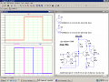
This is when both A and B are at 5V

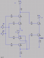
The base voltage of Q5 is 83 mV, the base voltage of Q6 is 1.9V, and the voltage at the emitter of Q5 and the collector of Q6 is 1.16V which makes absolutely no sense to me.

Any help would be appreciated!
 

Ylli

Joined Nov 13, 2015
1,092
Since Q5 is off, Q6 has no collector voltage. The Base-Emitter junction is acting like a simple diode, and the 'highs' on Q3/Q4 emitters passes through R9 and Q6 B-E junction.
 

crutschow

Joined Mar 14, 2008
38,574
  • Q5 is OFF so the collector of Q6 is an open circuit.
  • Q3 and Q4 are ON with an emitter voltage of about 4.3V at the left of R9.
  • Q6 has no collector current so R9's current goes through the base-emitter junction of Q6 and through R8 to ground, with a Vbe drop of about 0.7V, giving about 3.6V left over across R9 and R8.
  • Due to the voltage divider action, about 1/3 of this voltage appears across R8 or 1.2V (close to your observed 1.16V).
  • This voltage also appears at Q6's collector since the transistor is ON, making its collector and emitter voltages essentially equal (a transistor can conduct in either direction when ON).
  • Q6's base voltage is about 0.7V higher than its emitter or 1.9V, as you observed.
Make sense now?

So the circuit is working as built, but perhaps not as you intended. ;)
 

Thread Starter

drcne

Joined Aug 3, 2017
15
  • Q5 is OFF so the collector of Q6 is an open circuit.
  • Q3 and Q4 are ON with an emitter voltage of about 4.3V at the left of R9.
  • Q6 has no collector current so R9's current goes through the base-emitter junction of Q6 and through R8 to ground, with a Vbe drop of about 0.7V, giving about 3.6V left over across R9 and R8.
  • Due to the voltage divider action, about 1/3 of this voltage appears across R8 or 1.2V (close to your observed 1.16V).
  • This voltage also appears at Q6's collector since the transistor is ON, making its collector and emitter voltages essentially equal (a transistor can conduct in either direction when ON).
  • Q6's base voltage is about 0.7V higher than its emitter or 1.9V, as you observed.
Make sense now?

So the circuit is working as built, but perhaps not as you intended. ;)
Since Q5 is off, Q6 has no collector voltage. The Base-Emitter junction is acting like a simple diode, and the 'highs' on Q3/Q4 emitters passes through R9 and Q6 B-E junction.

Hey, thanks for the replies! What you guys are saying makes sense, but how is {Q5, Q6, R6, R8, R9, output} any different from an AND gate?
 

crutschow

Joined Mar 14, 2008
38,574
What I'm saying is this looks exactly like what I have on the right where my circuit isn't working correctly.

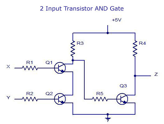
That will sort of work as an AND gate if the value of R is much larger than 1kΩ. That will minimize the feedthrough voltage with A is low and B is high.
The upper limit on R is determined by the current gain of the transistor.
 

Thread Starter

drcne

Joined Aug 3, 2017
15
Here's a better version:

Oh wow that actually works perfectly, thanks. One thing I noticed with my circuit was that the voltage dropped to about 3.3V after going through the gate. Why does the same thing not happen with this AND gate?
 

crutschow

Joined Mar 14, 2008
38,574
Oh wow that actually works perfectly, thanks. One thing I noticed with my circuit was that the voltage dropped to about 3.3V after going through the gate. Why does the same thing not happen with this AND gate?
Because there are no base-emitter voltage drops in the output path.
The output is a common-emitter transistor that is either fully-on saturated (output within a few mV of ground) or full-off (output pulled to the supply voltage by R4).
 
Top