hi,
You have calculated closely the period from the 5v level to the LOW transition, but is the question asking for the period between the High 3.5v and the Low 1.5 transition.?
hi,
You have calculated closely the period from the 5v level to the LOW transition, but is the question asking for the period between the High 3.5v and the Low 1.5 transition.?
Hi, thank for the reply.
The question is asking for the fall time under high to low transition.
I'm puzzle what the Low(1.5v) and High(5v) got to do with the value Vout.
Thanks.
hi.
The High and Low are the voltages at which a CMOS IC Logic input connected to Vo, senses as a High = '1' or a Low = '0' transition
It is assumed that Vo is the Logic output of a driving device, the value of 5V is a typical voltage.
If the Vo was say 5v and it was switched to 0v, the 5V 'charge' on the cap 5nF would discharge via the 1k resistor, exponentially. thru the 3.5v and 1.5v levels, towards zero.
Hi, Thanks for the reply.
Yes. I had understand the first 2 points, but still a bit unsure and confuse about the last line "exponentially. thru the 3.5v and 1.5v levels, towards zero.".
So I assume the Vout i will use to find the time would be the 3.5V instead of 1.5V, since it will be flowing through the capacitor then the resistor at 3.5v.
hi,
Look at this link, note the exponential nature of the capacitor discharge plot, it is not linear.
Your Vout [ capacitor voltage] is falling in the same way, it is not linear. http://www.electronics-tutorials.ws/rc/rc_2.html
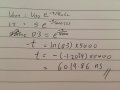
Your Vout starts at 5 V and falls exponentially to 0 V. That's not up for debate because that is the equation that the problem gives you.
The issue is what the transition time is defined to be? When do you start the clock? As soon as the voltage starts to fall? Or only once the voltage reaches the HI threshold of 3.5 V? The question of when you stop the clock is pretty clear. Stopping the clock with the voltage reaches zero is undefined because, mathematically, it never does. So you stop the clock when it reaches the LO threshold of 1.5 V.
So the only question we really have is when to start the clock. The problem doesn't make it clear which it wants, since both answer reasonable questions.
Q1) From the time this gate starts switching, how long will it take for the output to be recognized as a logic LO?
Q2) How long will the output of this gate be at an undefined logic level where it is neither HI nor LO?
So why not answer both of them? State the two different assumptions and provide an answer for each.
Hi Eric,
Thanks for simulating out the result. Easier for me to understand now hehe...
But about the question, I assume the question is asking me to get both the timing for 3.5v and 1.5v and get the differences.
Thank.
Your Vout starts at 5 V and falls exponentially to 0 V. That's not up for debate because that is the equation that the problem gives you.
The issue is what the transition time is defined to be? When do you start the clock? As soon as the voltage starts to fall? Or only once the voltage reaches the HI threshold of 3.5 V? The question of when you stop the clock is pretty clear. Stopping the clock with the voltage reaches zero is undefined because, mathematically, it never does. So you stop the clock when it reaches the LO threshold of 1.5 V.
So the only question we really have is when to start the clock. The problem doesn't make it clear which it wants, since both answer reasonable questions.
Q1) From the time this gate starts switching, how long will it take for the output to be recognized as a logic LO?
Q2) How long will the output of this gate be at an undefined logic level where it is neither HI nor LO?
So why not answer both of them? State the two different assumptions and provide an answer for each.
That's something you are going to have to get used to.
It is not uncommon when someone writes a problem for them to have a particular interpretation in mind and to not realize that there might be other ways to interpret the problem. I've certainly given problems like that myself and I have no doubt that I will do it from time to time going forward.
But it's far worse once you get out into the "real world" because you will be designing things for customers who themselves don't have a good idea of what the problem is -- if they did they might well not need you to solve it for them. It is frequently the case that the hardest part of the design is getting to a point where you and your customer actually agree on just what the problem is that needs to be solved and what an acceptable solution actually needs to do. So dealing with ambiguous homework problems is a good, albeit usually unintended, opportunity, to develop these skills.
So instead of going to your instructor and saying, "I don't know what you are looking for here, could you please explain it to me." Think about the problem and go to them and say, "I'm not sure I understand what you are looking for here. I think it might be this, or perhaps it is this. Is either one of these what you had in mind, or is it something else?" That will do several good things. Just thinking about possible alternate interpretations will help you develop useful skills. Presenting them to the instructor will demonstrate that you ARE thinking about the problem. It will also let the instructor see HOW you are thinking about them, which might let them realize how the problem might reasonably be interpreted differently or possibly get a glimpse into how you are misinterpreting the problem so that they can correct it. All of these things apply in spades once you are dealing with paying customers.
The way i would do this in real life is i would start with the normal voltage HIGH level with whatever load was connected and work from there. This would mean i would use the equation twice, once to calculate the time from t=0 to the time it takes to reach that normal level say t1, and again to calculate the time it takes to get to a level of 1.5v say t2, then subtract t2-t1 to get the logical fall time. This is because i might not expect the output voltage to always be at exactly 5v. But i could just start with the expected normal high level, and that would lead to the same result.
This problem seems similar because you will note that they mention the HIGH and LOW levels twice, and they seem to be inferring that they want the time between when Vout is HIGH and when Vout is LOW, so this would mean we would calculate t1 as the time from t=0 to the time it reaches the HIGH level, then calculate t2 as the time it takes to reach the LOW level, then subtract t2-t1 to get the fall time.
That's unless it is a trick question, but if we take it at face value then they bother to mention both the LOW and the HIGH state voltages so we might assume that has to be included in the reasoning needed to get the value they are looking for. If this wasnt the case, then they mentioned the value for Vout being HIGH for no reason at all except to throw the student off track. Also, often the logic high level is the minimum needed so they might want to use that for the calculation. This would entail the same calculation as if it was 3.5v to start but using the somewhat simpler equation as the simpler viewpoint, so the result would come out the same.
In other words, we either use Vdd as shown in the equation and include the 3.5v point, or we replace Vdd with 3.5v and go from there. When we replace Vdd with 3.5v it is as if we were using a real world value of the output high voltage, but we can calculate it another way and that is by keeping Vdd as 5v and including the 3.5v point as part of the calculation. So in the end either way we do it we are doing it as it might actually happen in the real world.
Without over-analyzing the situation, the problem simply says:
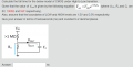
"Calculate the fall time for the below model under High (=3.5V) to Low (=1.5V) transition, given that Vout is defined by the following equation...."
Why is fall time in the CMOS transition region important? One may create possibilities, but is there really more than one way to interpret the problem statement?
Without over-analyzing the situation, the problem simply says:
"Calculate the fall time for the below model under High (=3.5V) to Low (=1.5V) transition, given that Vout is defined by the following equation...."
Why is fall time in the CMOS transition region important? One may create possibilities, but is there really more than one way to interpret the problem statement?
I think there are two reasonable ways to interpret it. Notice that it doesn't say that a HI = 3.5 V, only that 3.5 V this is the boundary of the region that is considered HI.
If you are told that the transition time for the output of a gate is 100 ns, what do you take that to mean, from a practical standpoint? I would take it to mean the time between when it starts transitioning until the time it reaches a defined LO. That is generally the more relevant parameter than how long it takes to transit the undefined zone, though this can be important, too (which it why that interpretation is also reasonable). Just imagine that, perhaps due to charge storage effects, it took 200 ns (making it absurd for emphasis) for it to get from the steady HI voltage of Vdd to the HI boundary and other 50 ns to get from there to the LO boundary. If you were a designer and you only got to know one number for the transition time, which would pick?
I took a quick look at a TI document and they choose neither -- their definition of transition time is the 10%-90% rise or fall time (and it's possible that this is how it is defined in the TS's case, just separate from the problem (since problems often expect students to apply course/text material that is not specified in every problem).
I still think the safest route, if clarification can't be gotten beforehand, is to simply solve the problem for both and indicated both interpretations on the homework. Even if the TS chooses to just use one interpretation and provide just one answer, I think they should cover their bet by noting that they are choosing a particular interpretation of the problem and mentioned other possibilities.
 Facebook
 Google
 GitHub
 Linkedin
 336.9 KB Views: 32