Facebook
 Google
 GitHub
 Linkedin
Hello Experts,
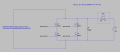
I have 2 SiC mosfets connected in a half bridge configuration.
Let call the top mosfet Q1 and the bottom mosfet Q2.
In parallel to this I have another half bridge connected in parallel.
Let call the top mosfet Q3 and the bottom mosfet Q4.
The Drain of Q1 and Q3 are shorted.
The Source of Q2 and Q4 are shorted.
The Source of Q1 is shorted to the Drain of Q2.
The Source of Q3 is shorted to the Drain of Q4.
And I have a resistive load connected at the midpoint of these 2 half bridges in between them.
I have a voltage source(Lets call this V1) connected as follows:
The positive terminal of the V1 goes to the drain of Q1 and Q3.
The negative terminal of the V1 goes to the drain of Q3 and Q4.
There is a capacitor bank in parallel.
At any time Either Q1,Q4 are turned OR Q3,Q2 are turned on.
The gate voltage given to these mosfets are (+15, -5).
With the above setup:
I am facing a weird issue, If V1 is disconnected and neither Q1,Q4 or Q3,Q2 are turned on,
if I measure across V1(across the H bridge), I measure about 20 to 22v? Why is this. Should it not be 0v?
PS: When posting this question to an AI chat bot , I got this reply below, Could you experts confirm this:
This voltage reading across V1 when neither Q1,Q4 or Q3,Q2 are turned on is likely due to the parasitic capacitances in the circuit.
When the MOSFETs are off, there is no current flowing through the resistive load, so any voltage on the parasitic capacitances can persist. The capacitances are charged to the voltage level of the previous switching cycle. When the voltage source V1 is disconnected, the voltage level on the parasitic capacitances is not discharged, and can be read as a voltage across V1.
To mitigate this issue, you can try to discharge the parasitic capacitances by shorting the output terminals of the half-bridge to ground or a neutral point (e.g. the midpoint of the two half-bridges) before measuring the voltage across V1. Another approach is to use snubber circuits to reduce the voltage transients and mitigate the effects of parasitic capacitances.