Understanding this Capacitor Charging Circuit

Thread Starter

gronkle

Joined Jun 2, 2012
18
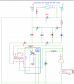
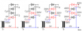
I have built a working capacitor charging circuit using a diagram that produces significant voltage at the electrodes and lights a torch. The circuit is based on a repurposed 1:50 step up transformer that is driven by a NPN transitor that oscillates the current.

I am a beginner, and I embarrassed to say that there are portions of this circuit that I do not understand even after staring at it for extended periods of time and need some help describing the function at a very basic level.

1. How does this circuit (B portion) oscillate to drive the transformer?
(please describe the stepwise relationship between P1/P2/Q1/C6/S1)
(I am especially interested in understanding the role of C6 in turning on/off Q1)
2. Why is R1 there?
3. Why is R4 in place?
4. What is the best way to measure the high voltage on C5? (I think it is near 4KV and don't want to blow my testor, and the C5 and R4 keep blowing out even though these components are stable on another circuit)

Thank you in advance. This forum has been very useful in the past.
 

Attachments

JDT

Joined Feb 12, 2009
657
I have only had a quick look but on your circuit diagram I think the base and collector are connected the wrong way round. Winding 1-2 5 is the driven winding and 3-4 is the feedback winding to the base. R1 is there to limit the base current. This circuit is a "blocking oscillator". Plenty of information about this on line.

R4 limits the output current in case of short circuits. C6 controls the rate-of-rise of the collector voltage (when the transistor is correctly connected) and basically protects the transistor. C6 works in a similar way to the "condenser" in olld IC engine ignition systems.

Be very careful measuring the output voltage as the charge on these capacitors could be lethal. THIS VOLTAGE COULD REMAIN FOR A LONG TIME AFTER THE CIRCUIT IS SWITCHED OFF. I would permanently connect a high value resistor in parallel with C5 to discharge the voltage when switched off. About 10M - 22M ohm would be good.

To measure, you need a voltage divider on your meter. This could be combined with your discharge resistor. For example if you use a 10k in series with 10M with the 10k connected to negative, this will give an approximate 1000:1 ratio. So 4V on the meter will indicate 4kV on the output.
 

Thread Starter

gronkle

Joined Jun 2, 2012
18
How can I change the transformer to draw it correctly? I disassembled the transformer to make the symbol. P1 is 15 turns and goes from pin 3 and 4...P2 is also 15 turns and goes between pin 1 and 5. S1 is ~750 turns of very light gauge wire and shares pin 5 with P2 and ends on pin 2.
 

Thread Starter

gronkle

Joined Jun 2, 2012
18
Thank you very much. I will research Blocking Oscillators.

I will check the attachments to Q1 and repost. (Weird thing is that the circuit already works on the board - perhaps I made the schematic wrong.)

I will be careful with this circuit. The capacitor dissapation portion of the circuit discharges the capacitor with a 10M resistor (R5) when the safety switch is applied (top of the second circuit diagram). The main capacitor is a Panasonic film capacitor (CAP FILM 0.33UF 630VDC RADIAL)...that incidentally keeps blowing out on occasion.

I will try a 10M/10k voltage divider tonight and repost. Do you have a recommendation on a wattage value for the resistors used? I am not certain how to determine the amps from a charged capacitor.
 

Thread Starter

gronkle

Joined Jun 2, 2012
18
Thank you JDT - I did the voltage divider and assessed that the charge on the C5 capacitor is 6kV (!)

After referencing the datasheet again - you were both correct, the NPN transistor symbol was incorrectly labeled, the corrected symbol is now in place, which makes the attachments to the transformer significantly different. (Funny - the circuit worked fine with the previous diagram...)

I have double checked the diagram - 1) does this still look like a blocking oscillator now...? (it no longer looks like it) (C6 is attached to the collector and the emitter, and I pulled apart the transformer to ensure the windings...phasings are still unclear)

Now that it no longer looks like a blocking oscillator...2) How does this thing oscillate? (can someone please describe the how P1/P2/Q1/C6/S1 work to make a square wave...)

3) What is the role of C6 now?

Lastly, 4) does anyone know a good way to turn the oscillator and Q1 off when the capacitor C5 reaches a set capacity (6kV) to save battery life?


Attachments

Last edited:

Dodgydave

Joined Jun 22, 2012
11,306
i think pins 1,5 need swapping on the transformer,the only way to stop the oscillator at a required voltage,is to use an opto coupler on the output using a Tl431 zener,then the opto will short out the Base/Emitter of the Q1,to stop it.
 
Last edited:

JDT

Joined Feb 12, 2009
657
Picture 1 looks good. The collector and base are connected correctly now.

To control the output, you need another transistor. This transistor should have its collector connected to the base of the driver transistor and emitters connected together. When this new transistor is off, the circuit works normally as before. Switching this transistor on will short the base of the driver transistor to 0V and stop the oscillator. Switch off, and it will run again. The base of this transistor needs to be driven by the output of a comparator, comparing a reference voltage (a zener diode, for example) with the output of the potential divider on the HV output.

So, when the output voltage gets to a certain voltage, the oscillator stops. When the voltage has fallen a bit, the oscillator will start again.
 

Thread Starter

gronkle

Joined Jun 2, 2012
18
JDT and Dodgydave - thank you very much, especially for the detailed descriptions that greatly aid in problem solving.

I will try out the output control circuit based on your suggestions and report findings and the new circuit diagram.

(I spent the evening last night looking for a "normally closed transistor" or PMOS depletion-mode FET to directly control VCC using a status signal from the high voltage...your solution is much easier)

In the educational spirit of this website:
Here is my current theory regarding why this oscillates: In the absence of polarity indicators, I assume that P1 and P2 are in opposite polarity directions just by looking at the diagram. As the power switch is turned on, 3VDC is delivered to P1 and current rises, this induces the first half of square wave current (1:50 = 150VAC) on S1 until the current flow stabilizes on P1. At the same time, the voltage passes through P1 and turns on Q1. As Q1 turns on and 3VDC is delivered to P2, the current flow rises in P2 (equal to P1 because the windings are equivalent)...but the process is slightly delayed by having to charge C6 first. The rise of current in P2 creates the inverse 150VAC square wave on S1. As the current rises in P2, this reverse biases P1, momentarily turning off Q1 starting the process over. I am guessing that the size of C6 controls the Hz rate.

Some of the connections still look unusual...so I will update the description as I continue to research it. I am going to review all circuit connections again (especially pins 1 and 5), but the circuit works as illustrated. I am also going to look for some equipment to observe the waves coming out of S1, P1, and P2 to further clarify observations...
 

JDT

Joined Feb 12, 2009
657
Transistor Q1 and the transformer form a "blocking oscillator". The frequency is determined by the properties of the transformer and to a lesser extent, C6.

When the circuit is first switched on, current in resistor R1 causes the transistor to conduct.
The inductance of the primary of the transformer causes the collector current to build up at a controlled rate.
As this current is increasing, induction causes a voltage on the base winding that adds to the base voltage, switching the transistor on more.
This continues until the magnetic field gets to a value where the core saturates.
The magnetic field can no longer increase.
No more induction so the induced voltage in the base winding falls to zero. The transistor switches off.
As the magnetic field collapses, the voltage on the base winding reverses. The transistor is fully switched off.
Capacitor C6 allows a current to continue flowing in the primary, controlling the rate of collapse of the field.
During this collapse, a high voltage is induced in the extra winding on the collector.
When the magnetic field reaches zero, the reverse voltage on the base winding becomes zero.
The sequence repeats.
 

Thread Starter

gronkle

Joined Jun 2, 2012
18
Thank you both very much for the help. I enjoy the learning experience.

JDT, that is a great description, I finally have a mental model on the thing.

I put the circuit on the oscilloscope and initial measurements indicating it is oscillating at 23kHz. Photo 2 shows P2, and a decent 5v AC-like waveform, driven by ~4v DC. Photo 1 is a measurement of S1, showing a comparable Hz-rate but a very odd waveform and voltage reading (18v peaks). I am going to go back and make sure I isolated the transformer from the Jacob's Ladder...maybe the reading is being affected by a capacitor I didn't disconnect...or maybe I had it hooked up wrong (it is a rat's nest currently)...that is certainly not what I expected it to look like. I will report the updated waveforms from P1, P2, and S1 driven by the transistor and then with a controlled waveform input on P1 and P2.

In either case, I think continual operation during the readings overheated and blew the transistor, which speaks to the importance of the comparator control circuit. I will work on this next and post results.

Dodgydave, I always welcome a technical head start, but I don't want to impose...
 

Attachments

Thread Starter

gronkle

Joined Jun 2, 2012
18
I have been messing with the comparator circuit driver to sense the state of the main capacitor via a voltage divider

output from c5 --> voltage divider to step down voltage --> comparator --> transistor to short out circuit driving the blocking oscillator

Since the point of this part of the circuit is 1) to protect Q1, and 2) to reduce power consumption of the battery powered circuit....is it advisable/possible to use a normally closed, depletion mode FET to shut off the power to the circuit instead of shorting Q1 ....when c5 is fully charged?

(This would seemingly save battery life in addition to Q1 health)
 
Top