Facebook
 Google
 GitHub
 Linkedin
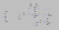
Hello , There is a very intresting circuit taken from the attached article.
I am trying to understand its mathemtical logic.
Could you help me logickally dissamble it into different parts so I will se the functionally of each part and how they play together?
https://www.edn.com/a-temperature-compensated-calibration-free-anti-log-amplifier/

I am trying to understand its mathemtical logic.
Could you help me logickally dissamble it into different parts so I will se the functionally of each part and how they play together?
https://www.edn.com/a-temperature-compensated-calibration-free-anti-log-amplifier/