TTL Logic problem Doubt

Thread Starter

Electronic_Maniac

Joined Oct 26, 2017
253
upload_2018-1-7_17-17-4.png

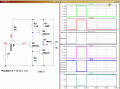
In the above standard TTL NOT gate, I am getting confused with the transistor Q1.

While solving for the status (ON,OFF) of the transistor Q1,

I would like to know what would be the Voltage at the base of the transistor Q1 (Input voltage at the emitter terminal of Q1=2.5V)
Can someone please help on how to find the voltage at the base of the transistor Q1 and the voltage across the 4k Resistor. Please.

Thanks in Advance.
 

Attachments

ScottWang

Joined Aug 23, 2012
7,501
There are two conditions that the one is the e of Q1 is connected to Gnd, and the other one is the e of Q1 is in series a 330Ω and connected to Gnd, if the Vbe_Q1 is 0.7V, now you can calculate the values of two conditions.
 

WBahn

Joined Mar 31, 2012
32,823
There are two conditions that the one is the e of Q1 is connected to Gnd, and the other one is the e of Q1 is in series a 330Ω and connected to Gnd, if the Vbe_Q1 is 0.7V, now you can calculate the values of two conditions.
Where are these two conditions coming from? If I'm reading the OP correctly, he was given that the voltage at the input (the emitter of Q1) was 2.5 V.
 

WBahn

Joined Mar 31, 2012
32,823
I tried. Is the value of the base voltage of Q1 = 1.8V ?
If the Ve of Q1 is 2.5 V and Vbe is 0.7 V (assuming the transistor is ON), then how is Vb = 1.8 V?

Vbe = Vb - Ve, so doesn't Vb = Ve + Vbe?

Now, there's a subtle point in this circuit, which is when the input is above a certain value, the NPN transistor gets functionally turned around and the emitter and collector are swapped. Do you see why?
 

ericgibbs

Joined Jan 29, 2010
21,439
Now, there's a subtle point in this circuit, which is when the input is above a certain value, the NPN transistor gets functionally turned around and the emitter and collector are swapped. Do you see why?
This 'reverse' transistor condition I was hoping he would realise or ask about from my post #5.
Hopefully he will come back.
E
 

ScottWang

Joined Aug 23, 2012
7,501
Where are these two conditions coming from? If I'm reading the OP correctly, he was given that the voltage at the input (the emitter of Q1) was 2.5 V.
Those were what I given him to thinking over the practical application, not just considered his original question, but he seems no interested about that.
 

Thread Starter

Electronic_Maniac

Joined Oct 26, 2017
253
hi EM,
Your Q1 Vb is close enough, is Q1 On or Off, when Q1 Ve =+2.5v... ?
E
That's what I am trying to figure out,sir! I want to know whether the transistor Q1 is ON or OFF?

My idea goes like this :

Since Q1 is NPN, if the voltage at the Emitter is greater than the base of Q1, Then Q1 will be reverse biased as Ve>Vb (NPN - Reverse bias condition)

So, I tried KVL on the outer loop, and I am getting 1.8V at Vb of Q1. Is it right?

And to all the people, I am just a beginner in Electronics, trying to solve a problem which happens to be simple for you. And I am not a native speaker of the English Language. So, I cannot understand any explanation or sarcasm unless it is explained in simple English.
 

Thread Starter

Electronic_Maniac

Joined Oct 26, 2017
253
If the Ve of Q1 is 2.5 V and Vbe is 0.7 V (assuming the transistor is ON), then how is Vb = 1.8 V?

Vbe = Vb - Ve, so doesn't Vb = Ve + Vbe?

Now, there's a subtle point in this circuit, which is when the input is above a certain value, the NPN transistor gets functionally turned around and the emitter and collector are swapped. Do you see why?
No sir. Can you please explain it ?

Thanks
 

WBahn

Joined Mar 31, 2012
32,823
No sir. Can you please explain it ?

Thanks
Consider that I have a block of silicon that in NPN with a contact to each region. Which is the emitter and which is the collector? In principle, it doesn't matter. In practice, they are generally design so that the characteristics for one choice are good at the expense of the characteristics for the other. But, even when that is the case, you can swap the emitter and collector labels on most NPN transistors and you still have an NPN transistor, just not a very good one. The base-emitter will still generally behave about the same as you would expect, but the transistor gain is generally very low.

So when you analyze a circuit and you discover that the voltage on the collector is less than the voltage on the emitter, you need to ask yourself if it is behaving like a transistor hooked up the other way.
 

WBahn

Joined Mar 31, 2012
32,823
That's what I am trying to figure out,sir! I want to know whether the transistor Q1 is ON or OFF?

My idea goes like this :

Since Q1 is NPN, if the voltage at the Emitter is greater than the base of Q1, Then Q1 will be reverse biased as Ve>Vb (NPN - Reverse bias condition)

So, I tried KVL on the outer loop, and I am getting 1.8V at Vb of Q1. Is it right?
How are you getting 1.8 V? Show us your work. We can't tell if your work is good or not unless you show it to us. More to the point, we can't tell you why it's not good unless we can see what you did.

If you got the 1.8 V by subtracting 0.7 V from the Ve of 2.5 V, then on what basis are you doing that? There is nothing that says that a reverse biased junction has 0.7 V across it.
 
Last edited:

Thread Starter

Electronic_Maniac

Joined Oct 26, 2017
253
How are you getting 1.8 V? Show us your work. We can't tell if your work is good or not unless you show it to us. More to the point, we can't tell you why it's not good unless we can see what you did.

If you got the 1.8 V by subtracting 0.7 V from the Ve of 2.5 V, then on what basis are you doing that? There is nothing that says that a reverse biased junction has 0.7 V across it.
Yes, sir. I did that only. And only after you told I realized what you said - "There is nothing that says that a reverse biased junction has 0.7 V across it."

So now, how can I find the base voltage? Please explain. Thanks
 

WBahn

Joined Mar 31, 2012
32,823
Yes, sir. I did that only. And only after you told I realized what you said - "There is nothing that says that a reverse biased junction has 0.7 V across it."

So now, how can I find the base voltage? Please explain. Thanks
Make an assumption for the mode of operation for Q1 and then analyze the circuit based on that assumption. Then check if the analyze shows that the device's resulting operating point is consistent with that assumption. If it isn't, then you guessed wrong. So pick another.

Let's say that you assumed that the transistor was on and in saturation. That would mean that the base voltage would be around 3.2 V (Ve + 0.7 V) and that the collector voltage would be about 2.7 V (Ve + Vcesat) and current would be flowing into the collector and out the emitter. Is that consistent with the rest of the circuit?

If not, pick a different mode and try again.

EDIT: Fixed typo (Vb should have been Ve).
 
Last edited:

Thread Starter

Electronic_Maniac

Joined Oct 26, 2017
253
Make an assumption for the mode of operation for Q1 and then analyze the circuit based on that assumption. Then check if the analyze shows that the device's resulting operating point is consistent with that assumption. If it isn't, then you guessed wrong. So pick another.

Let's say that you assumed that the transistor was on and in saturation. That would mean that the base voltage would be around 3.2 V (Vb + 0.7 V) and that the collector voltage would be about 2.7 V (Ve + Vcesat) and current would be flowing into the collector and out the emitter. Is that consistent with the rest of the circuit?

If not, pick a different mode and try again.
Sir, How are you saying,"base voltage would be around 3.2 V (Vb + 0.7 V) and that the collector voltage would be about 2.7 V (Ve + Vcesat)" .
I am getting what you are saying. can you please explain how is Vb=2.5V ? How you got 3.2V and 2.7V for base and emitter respectively?

Thanks
 

WBahn

Joined Mar 31, 2012
32,823
Sir, How are you saying,"base voltage would be around 3.2 V (Vb + 0.7 V) and that the collector voltage would be about 2.7 V (Ve + Vcesat)" .
I am getting what you are saying. can you please explain how is Vb=2.5V ? How you got 3.2V and 2.7V for base and emitter respectively?

Thanks
Typo on my part.

Meant to say Ve + 0.7 V. Ve is the given input of 2.5 V.

Sorry for the confusion.
 

Thread Starter

Electronic_Maniac

Joined Oct 26, 2017
253
hi EM,
In addition to WB's text, this LTSpice simulation of your circuit will help you visualise its operation.
I have made the assumption, that as it is a NOT gate, the Vi would be close to 0v, prior to the +2.5v input signal.

E
Thanks a lot! Really appreciate your help! Understood it clearly! :)
 
Top