routing strategy recommendations in ALTIUM

Thread Starter

yef smith

Joined Aug 2, 2020
861
Hello, I have tried to convert my schemtics into PCB (before polygon pour).
I got my traces looking very messy and its chaos.
DC +15 -15 was done on the buttom layer too.
I also need to do polygon pour after the traces will be ordered both on top and buttom layers ,the copper plates both will be GND net.
Printscreens of my schematics and pcb shown below.
My full project is attached in the link.
I'll be glad to have so tip and methods on how i can improve the routing in the project?
Thanks.

https://drive.google.com/file/d/1fSMrP67edmPFymSTFb0qWmbvB33Bv6_0/view?usp=sharing

1695992659531.png
1695992623746.png
 

jim_TX

Joined Jul 17, 2023
7
There is more to creating a design than just placing footprints onto the board and routing traces.
I posted a suggested Placement and routing on the Altium forum where you also post.
You have not taken into account the RF input connector (50 ohm impedance).
You have not taken into account the bypass capacitor placements.
You have not taken into account the routing of the V+ and V- voltage traces.
 

jim_TX

Joined Jul 17, 2023
7
The problem is that you are posting all over the place. You have started another new thread on the Altium forum, too.
It would make it easier for you to stay in one thread.
 

Thread Starter

yef smith

Joined Aug 2, 2020
861
Hello Jim,Yes i understand.
regarding the topics you suggested i will be

"You have not taken into account the RF input connector (50 ohm impedance)."
1. I have a connector with a 50 ohm width pad but R1 conecting to ithas much smaller width.(larger impedance)
my BW is 1MHz.do you reccoment doing a TAPER?
If you reccomend i'll be glad to know what proper taper is needed from connector pad width to R1 pad width.

You have not taken into account the bypass capacitor placements.
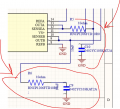
2.I have places a LPF filter on the outputs of the circuit to filter high frequency noise.
as shown in photo below.
What did i miss?
3. "You have not taken into account the routing of the V+ and V- voltage traces."
My V+ and V- are coming from the connector ,i tried my best to make it centralised.
Couldyou please reccomend me how to route properly V+ and V- ?
Thanks.
1696011481211.png
 
Top