rise of temperature on VIA at certain current and time pulse

Thread Starter

yef smith

Joined Aug 2, 2020
1,446
Hello,There is a demand for a delivery of 3 A through several layers using vias for 17.5 micro seconds.
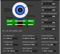
Presented below in the picture is my PCB manufacturer's abilities regarding vias.
A single via can withstand 1.4 A at shown bellow.
Is there some method to know what temperature rise i will get after 17.5 microseconds at 3A for such VIA?
Thanks.

1699385834764.png
 

ZCochran98

Joined Jul 24, 2018
351
That 1.4 A capacity (ampacity) comes from a maximum temperature change of 20 C (so 25 C -> 45 C). If you can tolerate higher temperatures, then that number goes up. If you were continuously carrying 3 A (or about 25-ish mW of power dissipated), then the temperature rise is closer to 92.
We can get these from the ampacity equations. For a wire or conductor completely exposed:
\[I = \sqrt{\frac{\Delta T}{R_{dc}\left(1 + Y_c\right)R_{th}}}\]
Here, \(R_{th} = \frac{\ln \left(r_2/r_1\right)}{2\pi L k}\) is the thermal resistance (\(L\) is the via length, \(r_1\) is drill radius, \(r_2\) is drill radius plus plating thickness, and \(k = 401 \mathrm{W\cdot m^{-1}K^{-1}}\) is the thermal conductivity of copper), \(R_{dc}\) is DC resistance (calculated the same way as thermal resistance, but with electrical conductivity \(\sigma\) instead of thermal conductivity \(k\)), \(Y_c\) is resistance from skin effect (if applicable), and \(\Delta T\) is the temperature change. In our case, \(r_1 = 0.0001\) m, \(r_2 = 0.00012\) m, \(R_{dc} = 0.00276 \Omega\), \(L = 0.0017\) m, so \(R_{th} = 0.04257\) K/W, which would get you a rise of 0.001 C. However, that's for an exposed conductor, and not one that's buried in a substrate. The copper-to-substrate thermal resistance will be much higher, so a better ampacity estimate comes from IPC-2221 calculations:
\[I = k \Delta T^bA^c\]
Here, \(k = 0.048\), \(b = 0.44\), and \(c = 0.725\), and \(A\) is the total via cross sectional area in square mils (making sure to exclude the hollow center). With this calculation at hand, we can calculate the maximum \(\Delta T\) for a given current:
\[\Delta T = \left(\frac{I}{kA^c}\right)^{1/b}\]
This evaluates to \(\Delta T = 93\) C, so about 118 C overall.

Now, all of this assumes that you're continuously carrying 3 A. If you are only pulsing your power for 17.5 us, then the total power dissipation will be much lower. As a rough estimate, if, over the span of \(t\) seconds you have the pulse on for \(t_p\) seconds, then your duty cycle will be \(\delta_t = t_p/t\), and your average power will be \(P_{avg} = P\delta_t\), so your "effective" current will be more like \(I_{avg} \approx \sqrt{\delta_t}I\), which will vastly reduce your temperature rise (very roughly, \(\Delta T_{pulsed} \approx \delta_t^{\frac{1}{2b}}\Delta T\) above). As a side note, pulsing like this is how we mitigate thermal problems in high-power RF amplifying applications.
 

Janis59

Joined Aug 21, 2017
1,894
I would guess the critical parameter is inductance. Every mm is 10 nH, the vias length 2 mm means 0.02 micro Henries. Thus all the calcs should begin with permitted inductance obtaining thus count of vias due inductance. And then recalc does this count is enough for heating. For heating aims the 5 A/mm2 is wonderful, but in case of well cooling textollite even 10 and probably 15 A/mm2 will not melt, however the 5 A/mm2 is in more secure zone.
 

Thread Starter

yef smith

Joined Aug 2, 2020
1,446
Hello ZCochan98, a very good explanation.
could you please explain how the temperature of a trace rises when i current pulse go threw it?
i have a very short pulse but a hught current and i am not sure if my trace could handle it.
If you could please give some theoretical besis on by how much my trace will heat when a pulse will go threw it?
Thanks.


That 1.4 A capacity (ampacity) comes from a maximum temperature change of 20 C (so 25 C -> 45 C). If you can tolerate higher temperatures, then that number goes up. If you were continuously carrying 3 A (or about 25-ish mW of power dissipated), then the temperature rise is closer to 92.
We can get these from the ampacity equations. For a wire or conductor completely exposed:
\[I = \sqrt{\frac{\Delta T}{R_{dc}\left(1 + Y_c\right)R_{th}}}\]
Here, \(R_{th} = \frac{\ln \left(r_2/r_1\right)}{2\pi L k}\) is the thermal resistance (\(L\) is the via length, \(r_1\) is drill radius, \(r_2\) is drill radius plus plating thickness, and \(k = 401 \mathrm{W\cdot m^{-1}K^{-1}}\) is the thermal conductivity of copper), \(R_{dc}\) is DC resistance (calculated the same way as thermal resistance, but with electrical conductivity \(\sigma\) instead of thermal conductivity \(k\)), \(Y_c\) is resistance from skin effect (if applicable), and \(\Delta T\) is the temperature change. In our case, \(r_1 = 0.0001\) m, \(r_2 = 0.00012\) m, \(R_{dc} = 0.00276 \Omega\), \(L = 0.0017\) m, so \(R_{th} = 0.04257\) K/W, which would get you a rise of 0.001 C. However, that's for an exposed conductor, and not one that's buried in a substrate. The copper-to-substrate thermal resistance will be much higher, so a better ampacity estimate comes from IPC-2221 calculations:
\[I = k \Delta T^bA^c\]
Here, \(k = 0.048\), \(b = 0.44\), and \(c = 0.725\), and \(A\) is the total via cross sectional area in square mils (making sure to exclude the hollow center). With this calculation at hand, we can calculate the maximum \(\Delta T\) for a given current:
\[\Delta T = \left(\frac{I}{kA^c}\right)^{1/b}\]
This evaluates to \(\Delta T = 93\) C, so about 118 C overall.

Now, all of this assumes that you're continuously carrying 3 A. If you are only pulsing your power for 17.5 us, then the total power dissipation will be much lower. As a rough estimate, if, over the span of \(t\) seconds you have the pulse on for \(t_p\) seconds, then your duty cycle will be \(\delta_t = t_p/t\), and your average power will be \(P_{avg} = P\delta_t\), so your "effective" current will be more like \(I_{avg} \approx \sqrt{\delta_t}I\), which will vastly reduce your temperature rise (very roughly, \(\Delta T_{pulsed} \approx \delta_t^{\frac{1}{2b}}\Delta T\) above). As a side note, pulsing like this is how we mitigate thermal problems in high-power RF amplifying applications.
 

ZCochran98

Joined Jul 24, 2018
351
Well, when the pulse is going through the via, as expected it will be dissipating power. But when the pulse is off, then it will radiate away the thermal energy it has gained. Let's say, for the moment, the pulse is a perfect square wave with "on" time \(T_{on}\), and the time between pulses is \(T_{off}\), for a total time (rising-edge-to-rising-edge) of \(T = T_{on} + T_{off}\), so the total ratio of ontime to total time is \(\delta_t = T_{on}/T\). The total energy that's dissipated into the via, if the thermal power is \(P\), will be \(E = PT_{on}\). But the total time between pulses is \(T\), so the amount of energy that's converted to heat is going to be \(E/T = PT_{on}/T = \delta_tP\). That's average power, which is significantly less than (assuming a low duty cycle - a small \(\delta_t\)) peak power.

Now, materials can only transfer energy in/out of the system so fast - thus thermal conductivity - and will heat up a certain amount in that time - measured partially by heat capacity. So you may have a large amount of current that, in steady-state (meaning thermally-radiated heat losses and thermal exchanges with the environment is balancing out the thermal energy being put into the via and surrounding material by the pulse) would be quite warm (about 118C, as calculated), but because that power is split over a long time, the via has longer to cool off than it has to warm up, so the effective temperature rise it will see is lower.

Ampacity and similar measures of how well a via or wire will survive current flow is measured on steady-state power flow. With pulsed scenarios, depending on the pulse, you can get away with far more than the rating would suggest.

This is how, in certain types of amplifier design, we can get away with, for example, tens or hundreds of watts of power output, but with minimal temperature rise - that enormous amount of power that a tiny chip is outputting (and, keeping efficiency in mind, means the DC power draw is probably twice as high) is in a super-short pulse, so the effective power that gets dissipated in the chip is significantly less.

Hope this answers your question!
 

Thread Starter

yef smith

Joined Aug 2, 2020
1,446
Hello ZCochran98, i have two questions regarding the great saturn tool and thetheory you presented:
1.my trace sits on 1.57mm dielectric ,its thickness is 2oZ so its 70um and width of 1.27
I have base copper and plate thickness parameters shown below marked by arrows.
what is the difference between this two because i am not sure where to put my 70um?

2.regarding this tool it assumes constant current not a pulse.
Is the some formula for a pulse going threw a trace?
Thanks.

1701241803483.png
 

Attachments

Janis59

Joined Aug 21, 2017
1,894
About the overheating vias - the best cure "on the fly" is just solder the wire in it.
Best method to indicate problem - thermo camera (Flir or another)
Only place the wire soldering may not help is path under the Nordic nRF-24 tablet, where the wires must be crossed and only available place is under the tablet. Thus there is no place for soldering but is place for via. (But it is enough with one, there). When it is not enough, the multiple parallel vias are applied customarily - take the same nRF Application Note and read about how many vias are demanded to printed antenna feed.
 

ZCochran98

Joined Jul 24, 2018
351
For your first question, the 70 um (2oz) is the total thickness. The base weight will contribute some, and the finish plating will contribute some. For this calculator, you can probably do 70 and 0 or 35 and 35 - that's up to you. If you're not sure, I'd stick with 70 and 0. The plating is from some final processing steps where the manufacturer will get some of the metal lost during etching back and thicken the metalization on the vias.

For formula for the pulse through the via, it is as I've discussed: if you know how long the pulse will be on and how long it will be off between pulses, you can estimate the temperature from the average power, rather than peak power. I'd have to do some more digging to see if there's a more concrete answer than that, but that's what I've used so far myself with sufficiently-satisfying results.
 

Thread Starter

yef smith

Joined Aug 2, 2020
1,446
Hello ZCochran98 ,sorry for the misunderstanding.my question is not about pulse current threw via but a pulse current threw a trace. The tool below calculates how much current the trace could handle .
Hoever its a continues current. I have very high current(twice the current recommended in the toll below) going threw the trace but for very short time.
if you could please elaborate about the case of a pulsed current going threw a trace with some period and duty cycle and see if he can handle it?

1701330413065.png
 

ZCochran98

Joined Jul 24, 2018
351
My bad! I misunderstood the question. Actual (non-buried) traces should be able to handle more current, as they can radiate heat out more. Based on the temperatures I see predicted for the continuous-current case in your screenshot, for pulsed applications the temperature should be lower, using the same average power rule-of-thumb I gave before. Using an older (IPC-2221) standard, we see the temperature rise formula is:
\[I = k\Delta T^{0.44}A^{0.725}\]
Here, \(I\) is current, \(k\) is a constant (0.048 for an external trace, 0.024 for an internal trace), \(\Delta T\) is your temperature rise, and \(A\) is your trace cross-sectional area in square mils (137.8 square mils, in your case). Rearranging gives:
\[\Delta T = \left(\frac{I}{kA^{0.725}}\right)^{2.273}\]
Checking this with your current (4.34 A) and the cross-sectional area gives a \(\Delta T = 8.3^\circ\)C, which is close to the predicted \(7.6^\circ\)C the calculator gave.
If our average power is, using the equation before, \(P_{avg} = \delta_t P\), then effective current, \(I_{eff}\) will be found in a similar way. Assuming the trace does not change impedance (not significantly) between pulsing and continuous, we have the following ratio:
\[\frac{P_{avg}}{P} = \frac{I_{eff}^2Z}{I^2Z} = \left(\frac{I_{eff}}{I}\right)^2\]
We know what average power is, so plugging it in gives:
\[\frac{\delta_t P}{P} = \left(\frac{I_{eff}}{I}\right)^2\]
\[\delta_t = \left(\frac{I_{eff}}{I}\right)^2\]
\[\rightarrow I_{eff} = I\sqrt{\delta_t}\]
So, you can use that to put into the temperature rise equation and it should get you a reasonably-accurate number. So, as an example with your current, if you have the pulse be a 1 ms pulse with a 9 ms pause, then \(\delta_t = 0.1\). That then lets us find the effective current: \(I_{eff} = 4.3\sqrt{0.1} \approx 1.36\,\mathrm{A}\). Throwing that into the IPC-2152 standard gives \(\Delta T \approx 0.6^\circ\)C. The IPC-2152 standard, which is considered to be more accurate, predicts closer to \(\boldsymbol{1.6^\circ}\)C instead. The reason I did not provide the IPC-2152 standard equation here is because it is given in terms of cross-sectional area and results in a nontrivial function to solve:
\[A = \left(117.6\Delta T^{-0.913} + 1.15\right) I^{0.84\Delta T^{-0.108} + 1.159}\]
I'm pretty sure that requires the Lambert W function to solve for \(\Delta T\) exactly, or some numerical method.
 

Thread Starter

yef smith

Joined Aug 2, 2020
1,446
Hello ZCochar98, from the Saturn tool shown below with 8mil width and and 2Oz thickness i get 20 degree rise with 1.37A of current.
my PCB is non buried.I am not sure if the tool uses buried or non buried trace dinition.
However i get using a tool 20 degree rise while in the formula you presented gives only 12.6 C.
Where did i go wrong implementing the formula ? why the tool gives a different result?
Thanks.

K=0.048
w=8; %width mil
t=2.75; %thickness 2Oz in mils
k=0.048;
A_mil_sq=w*t; %mil^2
I=1.3761;
delta_t=(I/(k*(A_mil_sq^0.725)))^2.273


1701768074157.png1701767001587.png
 

Attachments

ZCochran98

Joined Jul 24, 2018
351
Odd. I pulled up several calculators and each gave about 13ish degrees rise (calculators from Sierra Circuits, Qorvo, and Digikey). I'm not sure what your calculator is doing, as it looks like you have it set up correctly. I don't know what else to suggest here, as it seems to be an issue with the calculator, rather than your calculations.
 

Thread Starter

yef smith

Joined Aug 2, 2020
1,446
Hello ZCochar98 ,So if i understand corrctly i have few questions:
1.the formula for traces applies also for VIA's according to ipc-2221?
2.when i tried to put the numbers inside the unburied case of VIA i have:
Via hole of 8 mil's and plating thicknes of 0.7 mil ,so according to the photo below my annular area is 49 mil^2.
A=49
I=1.4
So i get a 3.49C temperature rise.
but in the Saturn tool it says 20C.
Where did i go wrong?

3.the IPC-2221 formula doesnt involve the VIA height parameter at all you have calcuated with this formula shown below but you said the its only for unburied case, Is there some formula for buried VIA's which takes into account the length of the via while its being buried?
Thanks.
1701798739696.png


1701796792485.png
1701792573117.png
3.regarding non buried Vias and buried VIA we have the situation described in the first post where my annual ring diameter

1701797851012.png

1701796418952.png
 

Attachments

Last edited:

ZCochran98

Joined Jul 24, 2018
351
Hello ZCochar98 ,So if i understand corrctly i have few questions:
1.the formula for traces applies also for VIA's according to ipc-2221?
2.when i tried to put the numbers inside the unburied case of VIA i have:
Via hole of 8 mil's and plating thicknes of 0.7 mil ,so according to the photo below my annular area is 49 mil^2.
A=49
I=1.4
So i get a 3.49C temperature rise.
but in the Saturn tool it says 20C.
Where did i go wrong?

3.the IPC-2221 formula doesnt involve the VIA height parameter at all you have calcuated with this formula shown below but you said the its only for unburied case, Is there some formula for buried VIA's which takes into account the length of the via while its being buried?
Thanks.
View attachment 309208


View attachment 309205
View attachment 309200
3.regarding non buried Vias and buried VIA we have the situation described in the first post where my annual ring diameter

View attachment 309207

View attachment 309203
1. I hadn't notice that, but it would appear so. That's odd. I suppose vias count as a kind of embedded line, though, so it somewhat makes sense.
2. In doing some digging through the resources I originally looked at, I noticed the value of \(k\) I had given was for external layers (my bad!). If we consider a via to be equivalent to an internal layer, then it should be \(k = 0.024\), roughly. Using this will give a temperature estimate of about \(27.2^\circ\mathrm{C}\), which is now too high (but better to be safe than sorry). A value of \(k\) that will match things exactly to some calculators I found online is \(k = 0.0274\). This makes qualitative sense: part of the via is exposed, so it's not as insulated as a fully-buried line, so \(k\) will be a bit higher than the buried line's, but most of the via is still buried, so it's not too much different. Saturn's tool uses IPC-2152, it seems, so it should give a more accurate prediction than the equation I provided.
3. In all the references I've seen for traces and vias, I've not yet seen one that incorporates via or trace length. That doesn't mean it's not out there, but IPC-2221 and IPC-2152 don't seem to care too much about it. Lengths are better used when you care about things like heat spreading or how fast it will heat up (due to thermal conduction). Here's one that summarizes IPC-2221 pretty well, and one that compares 2152 to 2221. I haven't found one that summarizes IPC-2152 in the detail I'm looking for yet.
 

Thread Starter

yef smith

Joined Aug 2, 2020
1,446
Hello ZCochar98 ,in Saturn when I lowered from 60 to 5 mil i got a loss of 3A in the ability of a trace to carry current threw it.
why PCB thickness plays a crucial role in the ability of a trace to pass current threw it?
Thanks.

1702972952435.png
 

ZCochran98

Joined Jul 24, 2018
351
That's odd. Unfortunately, I'm not sure why that would be the case for a DC line, unless they're assuming the back of the PCB is sitting on nothing (basically hanging in air). At which point, I suppose the heat calculation may be assuming the heat gets trapped in the PCB and cannot spread down and out as far? But that's the only thing I can guess at in this case.
 

jim_TX

Joined Jul 17, 2023
11
The difference may have to do with IPC-2221 & IPC-2152.
Here is the numbers with IPC-2221 selected.
1703267706795.png
To better understand it one would need to research the differences between the two specifications.

Also, it appears that this number may be just plugged-in and not calculated.
For example, from...
1 9mil = 1.7784 A
9-19mil = 2.1341 A
20-29mil = 2.5787 A
...and so on.
For further clarification on this it would probably be best to contact the author of the program to inquire the basis of the numbers.
 
Top