Facebook
 Google
 GitHub
 Linkedin
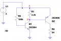
I could not complete the analysis of this circuit.

This is what I managed to do:
IB1 = (VCC - VBE1)/R3 = (3 - 0.7)/100K = 23uA
If β = 100, then IC1 = 2.3mA
VCE1 = VCC – IC1 * R1 = 3 – (2.3m* 2.2K) = - 2.06 V (Error)
The Voltage between points A & B (VAB) = 0.7 volt
So, IC1 = VAB/ R1 = 0.7/2.2K = 0.318 mA
Then, VCE1 = 3-0.7 =2.3 V
I stopped here. I wish I couldcalculate IC2 and VCE2 to complete the picture.
Thank you.