Facebook
 Google
 GitHub
 Linkedin
Project: How to make PCBs
- Thread starter Wendy
- Start date
Scroll to continue with content
Like Bill, I throw my chemicals away because they are cheap and in small volumes.
I'm doing photoresist now, so my developer is 2 teapsoons of NaOH in a liter of water - thrown away afterward (about 5 cents to make).
I etch with the same stuff Bill uses. H2O2 and HCl.
I buy H2O2 at the local Dollar tree for...surprise...$1.")
Local swimming pool supply sells muriatic acid (HCl) for $6 a gallon.
I mix 200cc of H2O2, 100cc of HCl - etch, and pour it on weeds in my back yard.
Good PCBs and no weeds!
I'm doing photoresist now, so my developer is 2 teapsoons of NaOH in a liter of water - thrown away afterward (about 5 cents to make).
I etch with the same stuff Bill uses. H2O2 and HCl.
I buy H2O2 at the local Dollar tree for...surprise...$1.
Local swimming pool supply sells muriatic acid (HCl) for $6 a gallon.
I mix 200cc of H2O2, 100cc of HCl - etch, and pour it on weeds in my back yard.
Good PCBs and no weeds!
I use ammonium persulphate and just keep adding more ammonium persulphate, HCl and hydrogen peroxide.
We're not allowed to pour any of this stuff down the drain. Eventually it goes to hazardous waste.
I don't tin my boards. If the copper is covered with photo resist, you can leave it on and the soldering iron will burn through it.
If I clean the board, I spray clear lacquer over the solder side after soldering.
You still have to be careful seal the acid bottle well, or like the FeCl the fumes will eat any metal near it. I generally pour a small quantity into a small polypropylene bottle similar to the peroxide bottle (label it well) to dispense small quantities. My use will be over a decade with the the acid, and hydrogen peroxide is literally available everywhere.
This thread has been a very interesting read on a chilly Saturday afternoon.
Finally my venerable stock of rub down etch resist transfers has perished. They won't stick to transparent film anymore, let alone pcb. So I turned to FreePCB to generate the artwork for UV exposure using an inkjet printer. I chose it because it is free, doesn't have any size limitations, and is good for use "on the fly", which cuts out a lot of the learning curve before you can get useable pcbs. A red felt tip pen on a hand drawn schematic as I go along is all the checking that I need for relatively simple boards.
However the big problem was getting prints onto film that were opaque enough for UV exposure. The default "bottom_copper.png" files produced by FreePCB are only 600dpi. The included command line app "GerberRender.exe" will produce 1200dpi png files, but even these gave rise to pin holes and cracks in the etched pcb when used to create artwork. Anything larger than 1200dpi caused it to run out of memory, even on this 6GB Ram laptop. I have tried printing twice, but found paper alignment to be too critical.
But Paintshop Pro, I use V8, has the abilaity to alter the dpi of a png image without altering the final size of the image, and by reducing the colours used from 256 to 2, to keep the image size to a minimum, a 2400dpi png can be achieved without memory shortage problems. These produce very opaque artwork and very clean etching.
My preferred transparent film is Jetmstar Premium, but even OHP inkjet film produces passable prints at this resolution, but they are nowhere near as durable. The ink seems to be absorbed into the surface of the Jetstar, but sits on top of the OHP and is easily accidentally scraped off.
Being a former Industrial Chemist I find the references to Muriatic Acid here very amusing. The existence of Murium, from which Muriatic Acid was made by dissolving the oxide of Murium in water, was bebunked in the 1780s, when it was discovered that this Murium Oxide was actually the element now known as Chlorine. Phlogiston was around at this time too. Now that was magic stuff, as it was thought for a while to have a negative weight before being debunked too. Technology certainly moves at a pace these days.
Nik
Last edited:
edwardholmes91
- Joined Feb 25, 2013
- 210
Firstly can I give a huge thanks to Bill for posting these fantastic, very detailed instructions! I have spent a very enjoyable last few hours picking up useful tips and reading through every post! It soon became apparent that without writing down my thoughts as I read through I would forget everything I wanted to say. Over two Post It notes later, I think I am ready to compose a reply with hopefully some useful hints and tips of my own too.
I have spent many happy hours making PCBs at school using the photoresist method and pre-sensitized boards, but the main problem that we always seems to have was the developing stage. Pupils struggled to strike the correct balance between over and under developing the board. We often noticed that the pre-sensitized boards had streaks on the edges of the coating even when we bought the premium quality FR4 board (as opposed to the SRBP (synthetic resin bonded paper) board, sometimes referred to as FR2). If overdeveloped the board would have pitted tracks and if underdeveloped it would be left with big copper blotches, which not only unsightly led to shorts in a lot of cases.
I noticed someone mentioned when using the photo board you can leave the coating on and solder through it. This is indeed true and it does protect the copper. Scouring pads can be used to remove this however the copper oxidizes and dulls very quickly, so I wouldn't advise it unless you are planning on plating the board. Don't get ripped off and buy the "photoresist strip" that they sell! I am pretty sure IPA (isopropanol) works just as well and I am positive that things like methanol work. I shy away from things like surgical spirit these days in favour of IPA because surgical spirit seems to leave an oily residue. Also don't confuse with turps (turpentine) this will definitely leave a residue unless washed with soapy water.
People have been asking about software. Personally I use Circuit Wizard which is made by a company called New Wave Concepts. I want to point out now, before I get a tirade of comments, it is primarily aimed for the EDUCATION sector. Therefore you may find its library of components, PCB routing, number of layers etc. limited compared with industry standard software. It does however simulate your circuit, showing current flow if required and voltage levels along wires. It converts schematics to PCBs either in single or double sided with a number of different configuration options. And it does allow you to use virtual instruments to test your PCB layout. On top of this you can do a check to check your PCB layout with the schematic. This means as long as the components are in the library there is no excuse for not checking your PCB before manufacturing!
Anyway, enough about expensive design software, lots of you have already mentioned lots of free programs that seem to have great capability. What I did want to highlight are a few programs that I find very useful and are FREE, these are:
PrimoPDF - It's a life saver. It will literally print anything. It installs as an extra printer on your computer and gives you a fair number of options when printing. There are also options to encrypt your PDFs if you wish.
Online Convert - I stumbled across this a few days ago whilst browsing the web and was very surprised with the vast array of files it will convert. Simply select your target file format and browse for the file you want to convert. Once you click go it will upload your file, process it and then serve it back to you as a download. I found an online PDF rotate facility too which is sometimes helpful but haven't yet found one that will invert or mirror. This isn't too much of a problem for me though because my PCB software has the facility to do this anyway.
Paint.NET - I've known about this for a long time, I'm told it is very similar to GIMP, but having never used GIMP myself I couldn't tell you. It is a very powerful program but it doesn't take an age to load like Photoshop used to (I say used to because before I upgraded my PC I could wait about 60 seconds or more for it to load... not however since I have built a bit of a beast of a PC with 16GB of DDR3 RAM it loads very quickly!)
I noticed a few people mentioned the Adobe Professional PDF viewer. I happen to be fortunate enough to own this (I got an Adobe package with significant student discount and it was included). One thing I will say is that you don't require PrimoPDF because Adobe has its own PDF printer. It also links into Microsoft Office for easy file conversion. Other than that though it isn't much different from the free version and personally it really IS NOT worth buying it unless you really really really need/want it!
Talking of PDFs, I know for certain Office 2007 onwards will allow you to save files as PDFs anyway in the little dropdown option for file type. This could also be a feature of older versions of Office but I can't remember (I didn't have cause for PDFs in those days... although I distinctly remember using Office 97 and being really happy when they brought out Publisher 98!)
Because of the cost mainly, of manufacturing presensitized boards when I decided to make some homebrew PCBs I went for the toner transfer method. Having never done this before I have to admit I was very pleased with the results.
A few things: I have a Samsung CLP 320 printer and I have to admit I am slowly starting to fall out with it. When I got it they sent me some print samples and the quality was excellent. I however can't seem to reproduce this same quality, I have been through the print settings time and time again with no luck. Not to mention the cost of replacement toner cartridges. Anyway I won't ramble on about it... a word of warning though, I DO NOT recommend it for printing heavy density artworks. Also note although it will print onto transparencies it doesn't work great and doesn't stick properly. (If anyone has this and knows how to increase print density please do let me know... I have set toner saving to 0% with no luck!).
So I decided to try a good old HP Color LaserJet 5M. This is a bit of a beast of a machine, very slow for processing large files and not great at high quality images. It does however produce very dense, reasonable quality artworks. Not to mention it cost £35GBP second-hand and came with literally a lifetimes worth of spare toner cartridges!
Toner transfer medium. I first tried using acetate because I had seen a YouTube video and the toner seemed to just peel off the acetate leaving it on the board. I was using a clothes iron with a piece of baking parchment in between the iron and the acetate. It was set to full heat and no steam. As the transfer wasn't 100% I used an indelible pen to fill in the bits that weren't 100%. This seems to work absolutely fine. I have seen etch resit pens but I can't make out if they are different to the same brand normal indelible pen. When I contact the customer support they said they that didn't know. What I do know is indelible pens work fine too.
With this transfer medium, obviously no water way needed to remove it. I have tried tracing paper but this just failed terribly. The best I have found so far it the backing paper that you get with some transparencies. It has an almost glossy side to it and this seems really good. But it does require a little bit of a soak in warm water for 10 mins or so to remove it carefully with a toothbrush. I am looking to try some baking parchment and also I'm told that old magazine paper works well. Still very much experimenting with the toner transfer method to be honest. Also worth noting that the board needs to be 100% clean, I find IPA good for this.
I etched the board using ferric chloride and warmed it up slightly before use. I know a lot of people are keen on the muriatic acid and hydrogen peroxide but I didn't know of this at the time and I figure that all the ferric chloride would last me a lifetime anyway. It says on the instructions to dilute by 30% so I have mixed up about 300ml of the stuff and I pour it into a separate similar container that is clearly labelled. I can keep using this until it is fully saturated and then dispose of it and mix some more up. So far I have etched 4 boards using it and not noticed any change in the time it takes to etch.
As pointed out it is very messy if you spill it and I would advise doing it outside for this exact reason. As of yet I haven't spilt any or stained anything but I best not speak too soon! I decided to get myself an etching tray that has a pouring spout. The reason I got this was because of the pouring spout and I can honestly say it makes pouring 100 times easier!
I will continue my post in another post as it seems I have hit the character limit
I have spent many happy hours making PCBs at school using the photoresist method and pre-sensitized boards, but the main problem that we always seems to have was the developing stage. Pupils struggled to strike the correct balance between over and under developing the board. We often noticed that the pre-sensitized boards had streaks on the edges of the coating even when we bought the premium quality FR4 board (as opposed to the SRBP (synthetic resin bonded paper) board, sometimes referred to as FR2). If overdeveloped the board would have pitted tracks and if underdeveloped it would be left with big copper blotches, which not only unsightly led to shorts in a lot of cases.
I noticed someone mentioned when using the photo board you can leave the coating on and solder through it. This is indeed true and it does protect the copper. Scouring pads can be used to remove this however the copper oxidizes and dulls very quickly, so I wouldn't advise it unless you are planning on plating the board. Don't get ripped off and buy the "photoresist strip" that they sell! I am pretty sure IPA (isopropanol) works just as well and I am positive that things like methanol work. I shy away from things like surgical spirit these days in favour of IPA because surgical spirit seems to leave an oily residue. Also don't confuse with turps (turpentine) this will definitely leave a residue unless washed with soapy water.
People have been asking about software. Personally I use Circuit Wizard which is made by a company called New Wave Concepts. I want to point out now, before I get a tirade of comments, it is primarily aimed for the EDUCATION sector. Therefore you may find its library of components, PCB routing, number of layers etc. limited compared with industry standard software. It does however simulate your circuit, showing current flow if required and voltage levels along wires. It converts schematics to PCBs either in single or double sided with a number of different configuration options. And it does allow you to use virtual instruments to test your PCB layout. On top of this you can do a check to check your PCB layout with the schematic. This means as long as the components are in the library there is no excuse for not checking your PCB before manufacturing!
Anyway, enough about expensive design software, lots of you have already mentioned lots of free programs that seem to have great capability. What I did want to highlight are a few programs that I find very useful and are FREE, these are:
- PrimoPDF - Used to print anything to a PDF file
- Online Convert - Converts literally hundreds of file formats
- Paint.NET - Similar to GIMP, a free graphics editing program with surprising functionality
PrimoPDF - It's a life saver. It will literally print anything. It installs as an extra printer on your computer and gives you a fair number of options when printing. There are also options to encrypt your PDFs if you wish.
Online Convert - I stumbled across this a few days ago whilst browsing the web and was very surprised with the vast array of files it will convert. Simply select your target file format and browse for the file you want to convert. Once you click go it will upload your file, process it and then serve it back to you as a download. I found an online PDF rotate facility too which is sometimes helpful but haven't yet found one that will invert or mirror. This isn't too much of a problem for me though because my PCB software has the facility to do this anyway.
Paint.NET - I've known about this for a long time, I'm told it is very similar to GIMP, but having never used GIMP myself I couldn't tell you. It is a very powerful program but it doesn't take an age to load like Photoshop used to (I say used to because before I upgraded my PC I could wait about 60 seconds or more for it to load... not however since I have built a bit of a beast of a PC with 16GB of DDR3 RAM it loads very quickly!
)I noticed a few people mentioned the Adobe Professional PDF viewer. I happen to be fortunate enough to own this (I got an Adobe package with significant student discount and it was included). One thing I will say is that you don't require PrimoPDF because Adobe has its own PDF printer. It also links into Microsoft Office for easy file conversion. Other than that though it isn't much different from the free version and personally it really IS NOT worth buying it unless you really really really need/want it!
Talking of PDFs, I know for certain Office 2007 onwards will allow you to save files as PDFs anyway in the little dropdown option for file type. This could also be a feature of older versions of Office but I can't remember (I didn't have cause for PDFs in those days... although I distinctly remember using Office 97 and being really happy when they brought out Publisher 98!)
Because of the cost mainly, of manufacturing presensitized boards when I decided to make some homebrew PCBs I went for the toner transfer method. Having never done this before I have to admit I was very pleased with the results.
A few things: I have a Samsung CLP 320 printer and I have to admit I am slowly starting to fall out with it. When I got it they sent me some print samples and the quality was excellent. I however can't seem to reproduce this same quality, I have been through the print settings time and time again with no luck. Not to mention the cost of replacement toner cartridges. Anyway I won't ramble on about it... a word of warning though, I DO NOT recommend it for printing heavy density artworks. Also note although it will print onto transparencies it doesn't work great and doesn't stick properly. (If anyone has this and knows how to increase print density please do let me know... I have set toner saving to 0% with no luck!).
So I decided to try a good old HP Color LaserJet 5M. This is a bit of a beast of a machine, very slow for processing large files and not great at high quality images. It does however produce very dense, reasonable quality artworks. Not to mention it cost £35GBP second-hand and came with literally a lifetimes worth of spare toner cartridges!
Toner transfer medium. I first tried using acetate because I had seen a YouTube video and the toner seemed to just peel off the acetate leaving it on the board. I was using a clothes iron with a piece of baking parchment in between the iron and the acetate. It was set to full heat and no steam. As the transfer wasn't 100% I used an indelible pen to fill in the bits that weren't 100%. This seems to work absolutely fine. I have seen etch resit pens but I can't make out if they are different to the same brand normal indelible pen. When I contact the customer support they said they that didn't know. What I do know is indelible pens work fine too.
With this transfer medium, obviously no water way needed to remove it. I have tried tracing paper but this just failed terribly. The best I have found so far it the backing paper that you get with some transparencies. It has an almost glossy side to it and this seems really good. But it does require a little bit of a soak in warm water for 10 mins or so to remove it carefully with a toothbrush. I am looking to try some baking parchment and also I'm told that old magazine paper works well. Still very much experimenting with the toner transfer method to be honest. Also worth noting that the board needs to be 100% clean, I find IPA good for this.
I etched the board using ferric chloride and warmed it up slightly before use. I know a lot of people are keen on the muriatic acid and hydrogen peroxide but I didn't know of this at the time and I figure that all the ferric chloride would last me a lifetime anyway. It says on the instructions to dilute by 30% so I have mixed up about 300ml of the stuff and I pour it into a separate similar container that is clearly labelled. I can keep using this until it is fully saturated and then dispose of it and mix some more up. So far I have etched 4 boards using it and not noticed any change in the time it takes to etch.
As pointed out it is very messy if you spill it and I would advise doing it outside for this exact reason. As of yet I haven't spilt any or stained anything but I best not speak too soon! I decided to get myself an etching tray that has a pouring spout. The reason I got this was because of the pouring spout and I can honestly say it makes pouring 100 times easier!
I will continue my post in another post as it seems I have hit the character limit
edwardholmes91
- Joined Feb 25, 2013
- 210
I would also like to point out that I use this board exclusively. I really don't like the FR2 that I mentioned earlier on and this stuff is a nice green colour I don't think it has been mentioned much on this thread, but I know a lot of people struggle cutting this board and don't want to have to buy expensive PCB guillotines. The method I tried seems to work great... mark on both sides the size of the board. Then using a sharp craft knife metal safety rule score nice and deeply into the board on both sides (be prepared to blunten your knife blade very quickly. I personally got a pack of 100 cheap blades from poundland and they work fine, they just wear quicker!) Once you have scored the board on both sides, clamp it to a workbench and snap along the line (be sure to clamp it right on the end and you get a nice clean break). You can then use a file to polish the edges a little although it is worth noting you shouldn't go breathing in the dust and may want to wear a dust mask. I had to remove about 5mm on one side of my PCB and so I got the trusty grinding wheel out and it ate through it like a hot knife and butter!
So I have talked about cutting the board, transferring the artwork and also the etching... perhaps I should have done it in a more logical order? Now comes the tin plating, this method isn't essential but I like the more 'pro' finish it gives, it helps protect the copper and it makes soldering a breeze! I bought these tin plating crystals. There is enough to mix a litre up but once mixed they have a shelf life so I decided to mix 1/3rd of them up and they work just fine. Again the board needed to be 100% clean to get good results with the tin plating. I use acetone at 99.5% to remove the toner and a non-abrasive scratchy sponge. Then once clean I use IPA to give another final good scrub before placing in the tin solution. Once in solution it will start plating before your eyes... it's actually kind of magical to watch! After minutes there should be a coating of 1 micron I think. Can't remember exactly but I know you don't want to leave the board in longer than required otherwise it gets thicker and thicker and will waste the solution.
I noticed a someone mentioned leaving the toner on the board while drilling and then removing it and tin plating after. This ensures that the tin is on the edge of the copper where the hole is drilled. It is something I have been meaning to do for a while and I keep forgetting to do it! Doh! Another thing I picked up on was people mentioned about the tin disappearing when soldering. This is unfortunately true, or certainly with the tin solution I use. I have found that the thicker the plating you give the board the more resilient it is. It seems to melt and mix with the solder. This isn't a problem but I think if you heat it less it doesn't happen as much.
A final note about drilling. It is absolutely essential IMHO to use a miniature drill in a drill stand if you want accurate holes and want to minimise the risk of breaking drill bits (put it this way, I have made a good few dozen boards over the years and not once broken a drill). Also make sure you don't apply too much pressure, let the drill do the work! If it is taking too long or the drill bit is getting too hot then you need to sharpen your drill bit!
I have had a Dremel Digital 400 for a long time now and never used it to drill PCBs because it wouldn't fit in my drill stand Recently I purchased one of these Dremel workstation drill stands and also one of these keyless chucks. The two fit together great and the mechanism on it is a really nice sprung rack and pinion. I read one review mentioning that it was poorly designed and plastic and that the instructions weren't clear. Admittedly there is some plastic but it is very well engineered and all I can say is what do you expect for £30GBP? The instructions aren't the clearest but seriously, who needs instructions for something this simple? If all else fails refer to the instructions surely? Not had chance to use it on a PCB yet but I can't wait because it has a lot less horizontal play and the action on it is so smooth!
Whilst on the topic of drills too. Don't even consider using HSS drill bits. I know you can get cheap sets in very small sizes and they are IMHO useless! My school used to use them to 'save money' and to be honest I think they ended spending more money replacing them because they snapped and became blunt so quickly than if they had of used better drills in the first place. The tungsten carbide drills are the way to go. I got myself a few 're-sharpened' ones and they worked fine for quite some time. Then the other day I had a bit of a spending spree and bought this tungsten carbide set. I have to admit I am very pleased with the investment, they are so sharp and they drill the FR4 a breeze. I'm beginning to think that the 're-sharpened' ones that I had missed being re-sharpened! This set is fine for holes up to 2mm which is more than enough for components but what about mounting holes and things like speaker grilles? I popped into my local hardware store and although they weren't able to give me any tungsten carbide drills I did get a set of cobalt drills from 1mm to 6.5mm and these are nice and sharp too. I think I wore out about 3 or 4 2.5mm HSS bits when drilling out holes for a speaker grille.
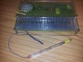
I will finish my very long ramblings with a picture of a board that I made:

If you are still reading at this point, then congratulations for your tenacity! I hope you have found some comments useful
I don't think it has been mentioned much on this thread, but I know a lot of people struggle cutting this board and don't want to have to buy expensive PCB guillotines. The method I tried seems to work great... mark on both sides the size of the board. Then using a sharp craft knife metal safety rule score nice and deeply into the board on both sides (be prepared to blunten your knife blade very quickly. I personally got a pack of 100 cheap blades from poundland and they work fine, they just wear quicker!) Once you have scored the board on both sides, clamp it to a workbench and snap along the line (be sure to clamp it right on the end and you get a nice clean break). You can then use a file to polish the edges a little although it is worth noting you shouldn't go breathing in the dust and may want to wear a dust mask. I had to remove about 5mm on one side of my PCB and so I got the trusty grinding wheel out and it ate through it like a hot knife and butter!So I have talked about cutting the board, transferring the artwork and also the etching... perhaps I should have done it in a more logical order?
Now comes the tin plating, this method isn't essential but I like the more 'pro' finish it gives, it helps protect the copper and it makes soldering a breeze! I bought these tin plating crystals. There is enough to mix a litre up but once mixed they have a shelf life so I decided to mix 1/3rd of them up and they work just fine. Again the board needed to be 100% clean to get good results with the tin plating. I use acetone at 99.5% to remove the toner and a non-abrasive scratchy sponge. Then once clean I use IPA to give another final good scrub before placing in the tin solution. Once in solution it will start plating before your eyes... it's actually kind of magical to watch! After minutes there should be a coating of 1 micron I think. Can't remember exactly but I know you don't want to leave the board in longer than required otherwise it gets thicker and thicker and will waste the solution.I noticed a someone mentioned leaving the toner on the board while drilling and then removing it and tin plating after. This ensures that the tin is on the edge of the copper where the hole is drilled. It is something I have been meaning to do for a while and I keep forgetting to do it! Doh!
Another thing I picked up on was people mentioned about the tin disappearing when soldering. This is unfortunately true, or certainly with the tin solution I use. I have found that the thicker the plating you give the board the more resilient it is. It seems to melt and mix with the solder. This isn't a problem but I think if you heat it less it doesn't happen as much.A final note about drilling. It is absolutely essential IMHO to use a miniature drill in a drill stand if you want accurate holes and want to minimise the risk of breaking drill bits (put it this way, I have made a good few dozen boards over the years and not once broken a drill). Also make sure you don't apply too much pressure, let the drill do the work! If it is taking too long or the drill bit is getting too hot then you need to sharpen your drill bit!
I have had a Dremel Digital 400 for a long time now and never used it to drill PCBs because it wouldn't fit in my drill stand
Recently I purchased one of these Dremel workstation drill stands and also one of these keyless chucks. The two fit together great and the mechanism on it is a really nice sprung rack and pinion. I read one review mentioning that it was poorly designed and plastic and that the instructions weren't clear. Admittedly there is some plastic but it is very well engineered and all I can say is what do you expect for £30GBP? The instructions aren't the clearest but seriously, who needs instructions for something this simple? If all else fails refer to the instructions surely? Not had chance to use it on a PCB yet but I can't wait because it has a lot less horizontal play and the action on it is so smooth!Whilst on the topic of drills too. Don't even consider using HSS drill bits. I know you can get cheap sets in very small sizes and they are IMHO useless! My school used to use them to 'save money' and to be honest I think they ended spending more money replacing them because they snapped and became blunt so quickly than if they had of used better drills in the first place. The tungsten carbide drills are the way to go. I got myself a few 're-sharpened' ones and they worked fine for quite some time. Then the other day I had a bit of a spending spree and bought this tungsten carbide set. I have to admit I am very pleased with the investment, they are so sharp and they drill the FR4 a breeze. I'm beginning to think that the 're-sharpened' ones that I had missed being re-sharpened! This set is fine for holes up to 2mm which is more than enough for components but what about mounting holes and things like speaker grilles? I popped into my local hardware store and although they weren't able to give me any tungsten carbide drills I did get a set of cobalt drills from 1mm to 6.5mm and these are nice and sharp too. I think I wore out about 3 or 4 2.5mm HSS bits when drilling out holes for a speaker grille.
I will finish my very long ramblings with a picture of a board that I made:
If you are still reading at this point, then congratulations for your tenacity! I hope you have found some comments useful
Attachments
-
 44.5 KB Views: 204
Last edited by a moderator:
Threads like this are very valuable, as they provide a wad of info to the newbie in homemade PCBs. Maybe too much of info.
I 'd like to do a wrapped up version of the thread, but I 'm not sure how to present it. Suggestions welcome.
I noticed that I hadn't contributed my experience on the subject, so here it is:
Method: Toner transfer
Paper: Medium weight laser photo paper. I have noticed that the better a paper transfers toner on the copper board, the harder it is to remove it before etching. Take your pick.
Software: Eagle. Very useful and customizable. Has a learning curve of about a week, though.
In the past, I used to print my .pdfs outside. On occasion, the masks would be scaled down by a small percentage. I have come to the conclusion that that was because the .pdf file was an A4 "image" that the printer tried to print on A4 paper. Acknowledging its margins, it would scale the design by a small about in order to fit it.
By cropping the .pdf edges and reducing the paper size, this problem was overcome.
Layer aligning (for two-layer boards): Currently I use an old, modified scanner to provide a light table. I cut the masks with a large-ish margin and asymmetrical "wings". I then align the two masks on the scanner and while I hold them down, I tape them together with paper tape. Ordinary plastic tape will melt under the iron and stick onto it. Generally, I avoid placing tape over the circuit.
The end result is an "envelope" where I slide the board inside.
Board preparation: Green scotch brite wire in moderation and isopropanol for finger oil stain removal.
Transfer Method: Household iron. Pre-heating the board helps, if possible. Be careful, as the mask will stick immediately onto a hot board. Always keep the iron flat and parallel to the board. Initially, I use the straight back of the iron to heat the whole mask and apply pressure. Then I use the tip of the iron to work on the whole of the surface again. In the end, the circuit should be clearly visible on the other side of the paper. When you think you are over, repeat the process at least two times over, for repeatable results of over 95%.
Removing the paper: This is the bottleneck for me. The paper I use really wants to stay with the toner. I dump the hot board on boiling water. I let it soak for 5 minutes and then peel the top layers of the paper by rubbing with my fingers. I soak it for another 2 minutes. Then, I use a plastic shoe brush to remove most of the remaining paper. The brush can be hard on the toner mask, so I work out the details with a toothbrush. In very narrow gaps between parallel traces, I resort to using a box cutter blade.
Etchant: Sodium persulfate grains, diluted as instructed in the box. I keep it in a glass beer bottle with a sealed plastic and rubber lid. I warm the etchant in the bottle over a camping gas stove for a few minutes, not to boil. I then pour it over the board in a small plastic container. I agitate for 5-15 minutes, depending on the freshness of the etchant. I have noticed that the particular brand I use can't etch more than 10-15 boards. I re-use the etchant.
I used FeCl once and will never do so again. Too messy.
Mask removal: Paper towel and white spirit. Haven't tried isopropanol yet.
Drilling: Black & Decker drill and drill stand. Extra choke for small bit sizes lets me go down to 0.5mm. Less than that and you can't thread wire through it. Never broke a bit yet.
Vias (for dual layer PCBs): I take two strands of multi threaded wire and twist them together with the drill, at about 30cm length. I solder one end through a via and put a little solder on the other free end for rigidity. Then, I stitch the wire through all the vias, without soldering yet. When the copper thread has run out, I solder the free end in the last via, to secure it and proceed to solder the vias in both sides. Finally, crop the thread going from one via to the other, to leave only the wires that connect both layers through a via. Usually one thread isn't enough, so repeat the process.
Finish: I use a plastic enamel spray to cover the boards. It reduces copper oxidation considerably, which can present itself as soon as a month later. It also gives a nice glittery finishing touch. However there is a dilemma. Apply it before soldering the parts, and the pads will get contaminated and harder to solder on. Apply it afterwards and you will cover your parts. This may or may not be an option to you.
Let me know if I forgot a step.
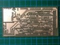
Here's an example of my work. The grid in the background is 1cm.
I 'd like to do a wrapped up version of the thread, but I 'm not sure how to present it. Suggestions welcome.
I noticed that I hadn't contributed my experience on the subject, so here it is:
Method: Toner transfer
Paper: Medium weight laser photo paper. I have noticed that the better a paper transfers toner on the copper board, the harder it is to remove it before etching. Take your pick.
Software: Eagle. Very useful and customizable. Has a learning curve of about a week, though.
In the past, I used to print my .pdfs outside. On occasion, the masks would be scaled down by a small percentage. I have come to the conclusion that that was because the .pdf file was an A4 "image" that the printer tried to print on A4 paper. Acknowledging its margins, it would scale the design by a small about in order to fit it.
By cropping the .pdf edges and reducing the paper size, this problem was overcome.
Layer aligning (for two-layer boards): Currently I use an old, modified scanner to provide a light table. I cut the masks with a large-ish margin and asymmetrical "wings". I then align the two masks on the scanner and while I hold them down, I tape them together with paper tape. Ordinary plastic tape will melt under the iron and stick onto it. Generally, I avoid placing tape over the circuit.
The end result is an "envelope" where I slide the board inside.
Board preparation: Green scotch brite wire in moderation and isopropanol for finger oil stain removal.
Transfer Method: Household iron. Pre-heating the board helps, if possible. Be careful, as the mask will stick immediately onto a hot board. Always keep the iron flat and parallel to the board. Initially, I use the straight back of the iron to heat the whole mask and apply pressure. Then I use the tip of the iron to work on the whole of the surface again. In the end, the circuit should be clearly visible on the other side of the paper. When you think you are over, repeat the process at least two times over, for repeatable results of over 95%.
Removing the paper: This is the bottleneck for me. The paper I use really wants to stay with the toner. I dump the hot board on boiling water. I let it soak for 5 minutes and then peel the top layers of the paper by rubbing with my fingers. I soak it for another 2 minutes. Then, I use a plastic shoe brush to remove most of the remaining paper. The brush can be hard on the toner mask, so I work out the details with a toothbrush. In very narrow gaps between parallel traces, I resort to using a box cutter blade.
Etchant: Sodium persulfate grains, diluted as instructed in the box. I keep it in a glass beer bottle with a sealed plastic and rubber lid. I warm the etchant in the bottle over a camping gas stove for a few minutes, not to boil. I then pour it over the board in a small plastic container. I agitate for 5-15 minutes, depending on the freshness of the etchant. I have noticed that the particular brand I use can't etch more than 10-15 boards. I re-use the etchant.
I used FeCl once and will never do so again. Too messy.
Mask removal: Paper towel and white spirit. Haven't tried isopropanol yet.
Drilling: Black & Decker drill and drill stand. Extra choke for small bit sizes lets me go down to 0.5mm. Less than that and you can't thread wire through it. Never broke a bit yet.
Vias (for dual layer PCBs): I take two strands of multi threaded wire and twist them together with the drill, at about 30cm length. I solder one end through a via and put a little solder on the other free end for rigidity. Then, I stitch the wire through all the vias, without soldering yet. When the copper thread has run out, I solder the free end in the last via, to secure it and proceed to solder the vias in both sides. Finally, crop the thread going from one via to the other, to leave only the wires that connect both layers through a via. Usually one thread isn't enough, so repeat the process.
Finish: I use a plastic enamel spray to cover the boards. It reduces copper oxidation considerably, which can present itself as soon as a month later. It also gives a nice glittery finishing touch. However there is a dilemma. Apply it before soldering the parts, and the pads will get contaminated and harder to solder on. Apply it afterwards and you will cover your parts. This may or may not be an option to you.
Let me know if I forgot a step.
Here's an example of my work. The grid in the background is 1cm.
Attachments
-
 322.6 KB Views: 56
edwardholmes91
- Joined Feb 25, 2013
- 210
Georacer, sounds good to me, I can't think of anything you have missed. I noticed you mentioned about heating the board up before applying the mask. As you mentioned, the one problem I have with this is you have to get on placed spot on first time, otherwise it messes your mask up.
I never knew white spirit removed the toner mask. I use acetone. I found someone on eBay that was selling 99.5%. I figure the stronger/purer it is the better. I'm fairly sure IPA doesn't do anything to the solder mask... or if it does it's very minimal. It just doesn't seem to react to it like acetone does.
I never knew white spirit removed the toner mask. I use acetone. I found someone on eBay that was selling 99.5%. I figure the stronger/purer it is the better. I'm fairly sure IPA doesn't do anything to the solder mask... or if it does it's very minimal. It just doesn't seem to react to it like acetone does.
Actually, removing the toner mask is another thing I try to perfect. Previously I used to apply white spirit onto paper towels and scrub the board. That took a long time and strength to the point that my fingers hurt.
After that, I tried with a toothbrush in a shallow cup. Toner diluted in white spirit splashed everywhere.
Lately, I try to soak the board in white spirit in a closed tupper, shake it for a while and then scrub it. The toner gets off of the board more easily then, though it's still a slightly messy process.
edwardholmes91
- Joined Feb 25, 2013
- 210
Georacer, I place the board in the utility sink. Pour acetone on it and let surface tension hold on on the surface of the board. Leave it a few minutes then I use an old non abrasive kitchen scratchy pad. Works a treat, just need to make sure you remove every last trace of it from the sink because it you leave some once the acetone dried you will be left with bits of toner stuck to your sink and have to clean it with acetone.
Dr.killjoy
- Joined Apr 28, 2013
- 1,196
What's a utility sink? I bet I don't have one in my house.

I use nail varnish remover (aka acetone) to remove photoresist after etching. Works a treat. Just tried it on toner (on the transparency I used for photoetching) and it removes it pretty easily. It's ridiculously cheap, but you get funny looks in the shop.
Not if you enter singing the "lumberjack" song.
edwardholmes91
- Joined Feb 25, 2013
- 210
Haha, that's why I got my Mum to go and buy it for me instead... although I have just bought 1L of 99.5% pure acetone from eBay so I am keen to try it to see how well it removes it compared to the nail varnish remover. I think the keep is to let it soak a little while and that will let it soften up nicely.Not if you enter singing the "lumberjack" song.
Did you know toner is actually mainly made of plastic mixed with a wax to give it the shiny glean? Styrene acrylate copolymer is commonly used amongst other materials.
Regarding the utility sink... I mean not your kitchen sink basically... unless you want your parents or partner going crazy at you!
Last edited:
edwardholmes91
- Joined Feb 25, 2013
- 210
I haven't seemed to be able to find it in the UK, but it was fairly easy to pick up off eBay. I think I paid about £10 for 1L of it. Probably a little too much in reality but I've got enough to last me a lifetime now anyway!Acetone is not hard to get, the local hardware stores have it.